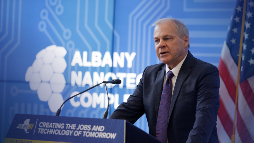
“On behalf of NY CREATES, I would like to extend our congratulations to Arizona State University on being selected as the anticipated location for the CHIPS for America NSTC Prototyping and National Advanced Packaging Manufacturing Program (NAPMP) Advanced Packaging Piloting Facility, an NSTC and NAPMP facility. We welcome ASU as a critical peer supporting the NSTC’s mission, as NY CREATES hosts the CHIPS for America EUV Accelerator, a flagship NSTC facility at our Albany NanoTech Complex, North America’s most advanced non-profit semiconductor R&D center. Together, our collective efforts will drive transformative innovation, strengthen the U.S. semiconductor ecosystem, and ensure our nation’s leadership in next-generation technologies. We look forward to collaborating with ASU, Natcast, and the broader network of partners to advance the future of microelectronics.”
-Dave Anderson
NY CREATES President

Biden-Harris Administration Announces Arizona State University Research Park as Planned Site for Third CHIPS for America R&D Flagship Facility
Facility is expected to host the world’s first 300mm front-end semiconductor manufacturing and advanced packaging research facility
Today, the Department of Commerce and Natcast announced the Arizona State University (ASU) Research Park in Tempe, Arizona as the anticipated location for the third flagship CHIPS for America research and development (R&D) facility. The CHIPS for America NSTC Prototyping and National Advanced Packaging Manufacturing Program (NAPMP) Advanced Packaging Piloting Facility (PPF), an NSTC and NAPMP facility, will feature cutting-edge capabilities to bridge the gap between laboratory research and full-scale semiconductor production. It will enable researchers and industry leaders to develop and test new materials, devices, and advanced packaging solutions in a state-of-the-art R&D environment. This newly constructed facility is expected to be operational in 2028 and will play a key role in driving U.S. leadership in semiconductor innovation, economic growth, and national security.
“A strong research and development ecosystem is essential to ensuring the United States remains at the forefront of semiconductor innovation,” said U.S. Secretary of Commerce Gina Raimondo. “Arizona has long been a hub for technological progress, and this new facility will strengthen our domestic supply chain, drive advanced manufacturing breakthroughs, and secure America’s leadership in this critical industry. Thanks to the bipartisan CHIPS and Science Act, combined with the other two CHIPS for America R&D flagship facilities, we will help bring American innovations to the global market, further securing our national and economic security.”
“Thanks to the bipartisan CHIPS and Science act, we are investing at historic levels in the technologies of both today and tomorrow,” said White House Deputy Chief of Staff Natalie Quillian. “Today’s announcement with ASU ensures the United States will continue to be a leader in research and development and win the future by investing in skilled workers, moonshot technologies, and the advancements needed to stay ahead in critical industries, such as AI.”
Scaling new semiconductor technologies from research to full production remains a significant challenge for the industry. Key obstacles include a lack of 300mm semiconductor wafer prototyping capability facilities and the absence of shared access to specialized facilities, shared infrastructure, skilled resources, and capital.
To meet these challenges, CHIPS for America is investing in integrated R&D activities to fill a critical gap in the lab-to-fab innovation cycle. The PPF’s prototyping capabilities will consist of at least one 300mm full-flow complementary metal-oxide-semiconductor (CMOS) technology as a stable baseline for experiments. The facility will also allow for a variety of R&D in a manufacturing-like environment that would not be feasible at a manufacturing site, including novel materials and device architectures. Key packaging capabilities are expected to include a baseline advanced packaging piloting line to enable the development and commercialization of new packaging processes. The facility will also support U.S. workforce development efforts by providing opportunities for collaborative, hands-on research utilizing industry-leading tools and equipment.
“The PPF will play a critical role in advancing semiconductor innovation across the country,” said Deirdre Hanford, Natcast CEO. “This facility will be a premier destination where researchers from industry, academia, startups, and the broader semiconductor ecosystem will convene to explore, experiment, and collaborate on the next generation of semiconductor and packaging technologies that will power the industries of the future.”
As one of three CHIPS R&D flagship facilities, the PPF will be amplified by Arizona’s robust and growing microelectronics landscape, including leading front-end semiconductor manufacturing and advanced packaging companies, and a vibrant university research environment. The expected partnership with ASU will jumpstart R&D in these areas and leverage the substantial programs underway at the university.
Combined with the EUV Accelerator and the Design and Collaboration Facility, these state-of-the-art flagship facilities will establish world-class destinations for advanced semiconductor R&D in the United States. They will address critical gaps in the current ecosystem, offering unparalleled value to a diverse array of stakeholders across the semiconductor value chain, including universities, small businesses, large manufacturers, and government agencies, and help build vibrant semiconductor ecosystems in the U.S. that bolster cutting-edge R&D and create quality jobs. The Department of Commerce and Natcast expect to announce information in the coming months about the process for selecting affiliated technical centers.
Natcast has accepted a nonbinding Letter of Intent from the Arizona Commerce Authority and Arizona State University. The final contract is subject to additional due diligence, continued negotiations, and refinement of terms.
CHIPS for America and Natcast announced the model and selection process for the three CHIPS R&D flagship facilities in July 2024. The selection of these sites followed a multi-phase facilities selection process and is consistent with the July 2024 facilities model, which was informed by more than a year of discussions with stakeholders building on the release of the NSTC Vision and Strategy paper and the NAPMP Vision paper as well as robust analysis on the current and planned future state of the U.S. semiconductor manufacturing and R&D ecosystems. A request for information published by Natcast in March 2024 also collected feedback on the demand for prototyping facilities capabilities and informed the facility model.
Learn more about the CHIPS for America R&D flagship facilities and other NSTC initiatives at natcast.org.
