This ecosystem has enabled small- and medium-size businesses, which would otherwise be priced out of the market, to bring integrated photonic chip (IPC) technologies through the product development cycle. Members (there are over 120) and partners can use the resources provided by AIM without incurring prohibitive costs or risking more than they can afford. AIM’s test assembly and packaging (TAP) facility in Rochester, N.Y. — one of the organization’s primary achievements during its first five years — is the only 300-mm photonic packaging research facility in the world with open access.
“The test assembly and packaging facility is key to advancing the technology,” Ed White, AIM Photonics associate vice president and National Photonics chair, said. “Allowing companies to have access to the means to get their photonics product to market is something that doesn’t exist anywhere else in the world, except in privately owned facilities.” The cost of developing a chip is very high, and assembly and packaging easily make up one-half of that cost, White said.
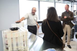
Ed White (left), associate vice president of AIM Photonics TAP facility and National Photonics Initiative chairman, describing how a 300-mm wafer is tested in the analytical lab.
The TAP facility makes it possible for small companies that may need only one chip on a wafer to develop and produce only what they need. “We help them get in the game by giving them access to very expensive technology,” White said. “Their minimum run can be what they need it to be — one chip or 10 or 50. We can provide the means to package for as many or as few wafers as needed.” TAP has development and production process capabilities in wafer scale, chip scale, and I/O attach. The facility has state-of-the-art test and metrology capabilities for each of these functional areas.
AIM’s IPC development team in Albany, N.Y., is available to help AIM Photonics members with their IPC designs. The photonics member community can access design libraries created by AIM and then transfer that design to the chip development team in Albany. After the PIC is made, it’s transferred to the TAP facility for final test, assembly, and packaging.
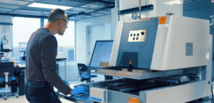 AIM Photonics TAP engineer testing wafer in the analytical lab.
The AIM ecosystem — composed of the Process Design Kit (PDK), Multi Project Wafer (MPW), private and custom wafer runs, and the TAP facility — has led to significant advancements in PIC technologies over the past five years. “Many industry, government, and academic partners have stated that without the ecosystem, some of the current advancements would not have been possible for another five to 10 years,” Frank Tolic, chief marketing officer, said. Developments facilitated by the AIM ecosystem during its first five years include quantum photonic chips; advances in biomedical and biochemical sensors; optical transceivers that today perform at the speed of 400 to 800 Gb, and that in the future will perform at Tb speed; radio frequency (RF) over fiber applications; and lidar on a photonics chip.
Photonics in the Time of COVID
By drawing on its experience in managing product timelines and scaling production, AIM Photonics was able to respond quickly to the pandemic, submitting a proposal to the U.S. Department of Defense (DoD) to be one of the first to support research in testing for the SARS-CoV-2 virus. AIM is helping industry, the DoD, and research labs collaborate on sensors for the testing, with the goal of having new sensors on inexpensive silicon chips by 2020-2021 flu season. While initial commercial rollout will be to clinical laboratories, the ultimate goal is to have a point-of-care SARS-CoV-2 test for use wherever flu tests are offered. AIM is facilitating a collaboration between the University of Rochester and Ortho Clinical Diagnostics to develop sensors for SARS-CoV-2 testing, and is partnering with researchers at SUNY Polytechnic Institute on the development of microfluidic devices for use in testing for SARS-CoV-2.
Helping Lockheed Realize RF over Fiber Solutions for Its Platforms
Lockheed Martin is working with AIM Photonics to improve RF over a fiber network. Integrated photonics will allow the company to use more compact chips, reducing size and weight and saving power. IPCs will give its data communications more bandwidth and scalability. The business will be able to respond to new requirements quickly, without the need to re-cable, by moving existing fiber cabling to a different frequency and using multiplexing to put multiple sources of information on a single fiber. Lockheed has been a member of AIM Photonics since 2017.
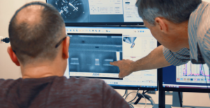
Engineers analyzing AIM Photonics device structures in chips at TAP analytical lab.
AIM is working to extend its funding agreement with the DoD and the contracting process it uses in support of the congressional plus-up program. New York State has made a strategic investment in AIM Photonics, providing $250 million in funding. “A large portion of that was spent on the TAP facility in Rochester, on new metrology tools and equipment that is now being used by our members,” Tolic said.
In the next five years and beyond, AIM will seek to advance the IP ecosystem it has created through continued collaboration with its members and partners. Some existing and new technologies that AIM will focus on could include new PDKs for specific technologies such as sensors, packaging, and quantum. AIM will continue to welcome and support new ideas and collaborations from industry, academia, and government. It also intends to expand educational programs for PIC technology and applications, with a focus on expanding these programs to community colleges and undergraduate programs across the U.S.
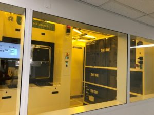
Recently installed new equipment at Rochester, N.Y., TAP facility.
The AIM Photonics TAP facility continues to engage with existing and future clients. The TAP facility is currently engaged with more than 20 customer projects and is in discussions with a number of other organizations about future work. The interest in the AIM Photonics TAP facility is high among the photonics community. “Nearly half of the people who visited us at the last nonvirtual conference, Photonics West 2020, had a primary interest in the AIM Photonics TAP facility,” Tolic said. “We are working with several Rochester-based companies and universities, including Ortho Clinical, Syntec, L3Harris, Mosaic, UR, and RIT, and new companies are looking to work with us, especially in the areas of sensors and datacomm.”
If you are interested in learning more about how the AIM Photonics ecosystem can help you bring your idea for a photonics product to market, visit http://www.aimphotonics.com/info-request. Your information will go directly to the AIM Photonics business development team.
ROBIN RILEY, WEB EDITOR
ROBIN.RILEY@PHOTONICS.COM
https://www.photonics.com/Articles/At_5-Year_Mark_AIM_Photonics_Looks_Back_on_Key/a65863
Photonics.com
Jun 2020