


Read Governor Hochul’s Press Release Here
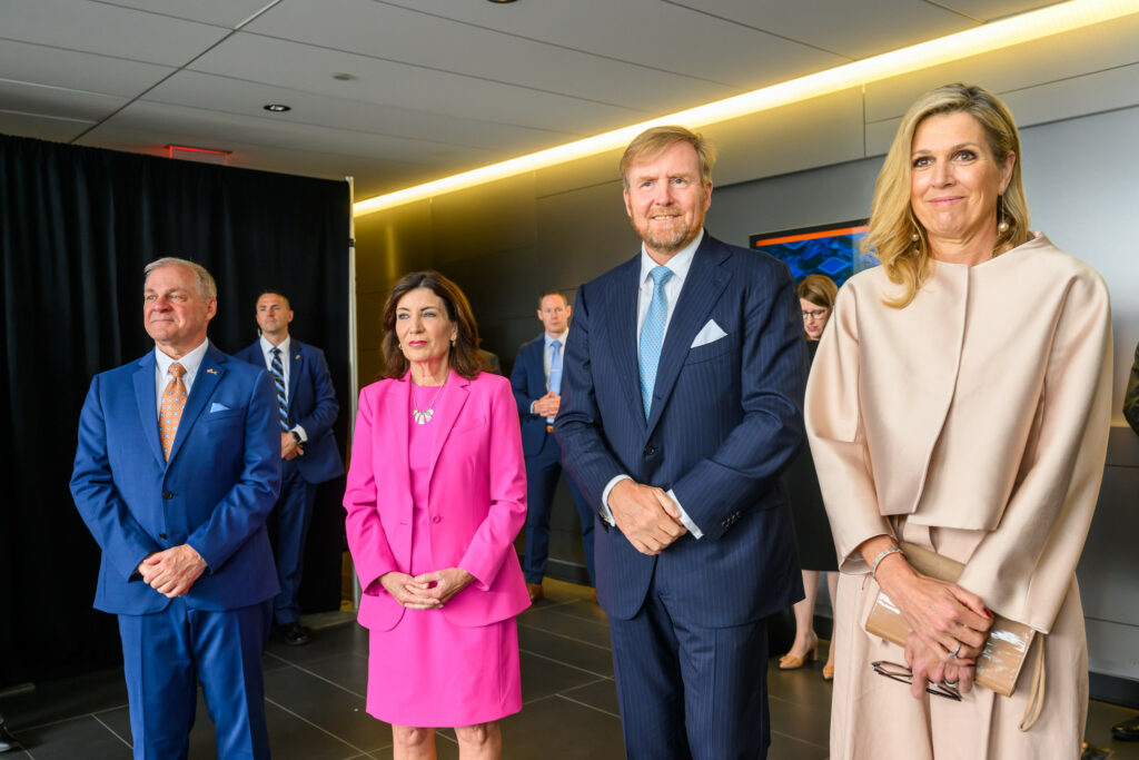
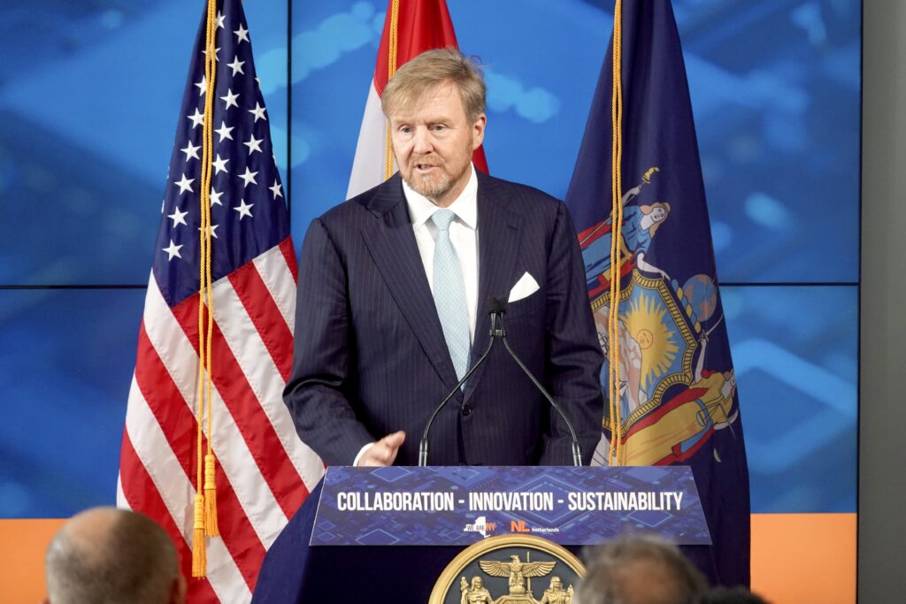
During Royal Visit by Their Majesties King Willem-Alexander and Queen Máxima of the Netherlands, Governor and Netherlands Minister Sign Memorandum of Understanding To Advance Shared Goals for the Future of Semiconductor Manufacturing
Establishes New Program To Sponsor up to Five SUNY Students’ Attendance at Prestigious Eindhoven Semicon Summer School Program in the Netherlands
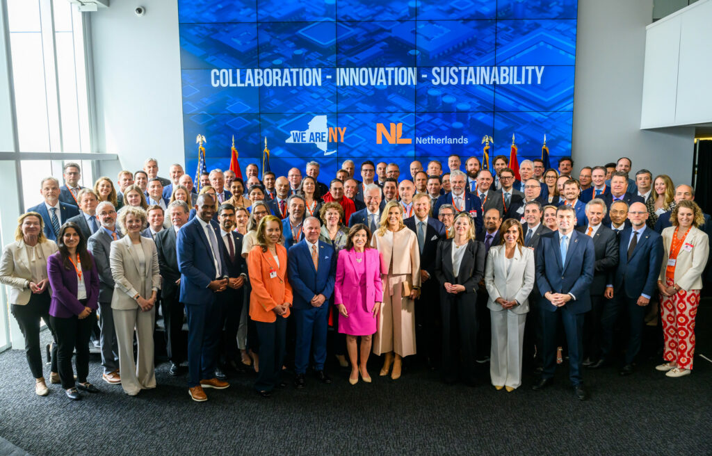
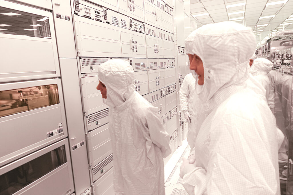
Governor Also Hosts NY/Netherlands Semicon Forum at NY CREATES’ Albany NanoTech Complex to Convene Semiconductor Businesses, Researchers and Supply Chain Partners
Builds on Governor’s Commitment to Creating a Modern, 21st Century Economy in New York State
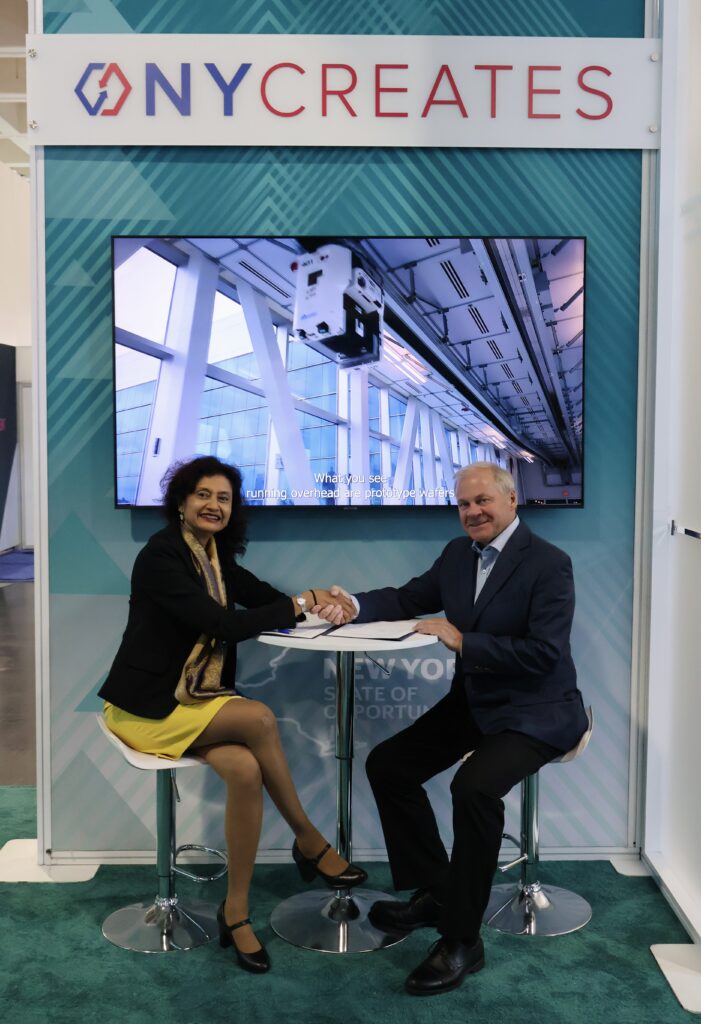
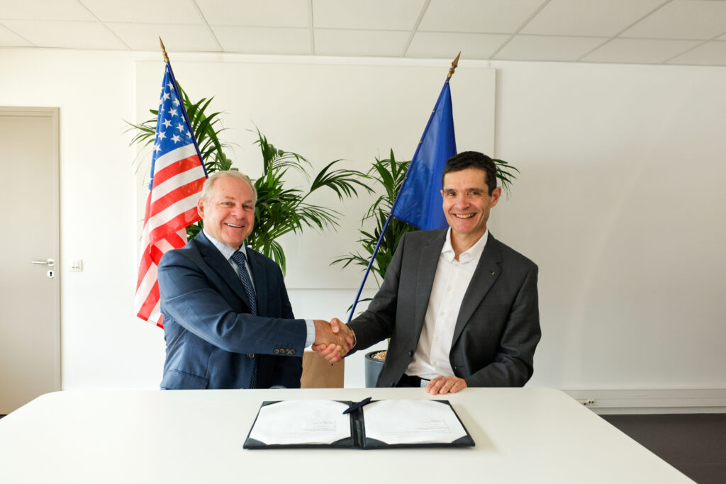
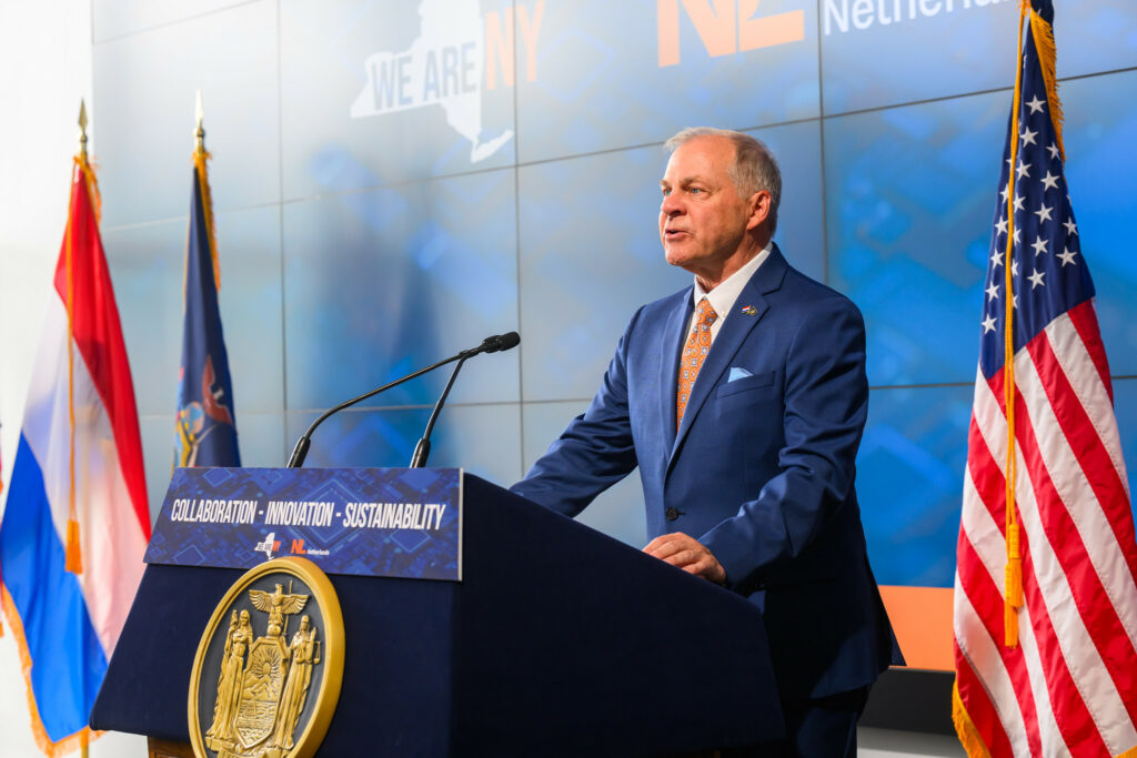
Governor Kathy Hochul and Netherlands Minister for Foreign Trade and Development Cooperation Liesje Schreinemacher today announced a new partnership to strengthen innovation and collaboration in the semiconductor industry between the Netherlands and New York State during the royal visit by Their Majesties King Willem-Alexander and Queen Máxima of the Netherlands. The partnership, formalized in a memorandum of understanding signed today by Governor Hochul and Minister Schreinemacher recognizes the entities’ shared interest in promoting sustainability within the semiconductor industry, enhancing joint workforce development opportunities, and advancing semiconductor research and development. As part of this new partnership, the Governor also announced a new state program to sponsor up to five SUNY students’ attendance at the prestigious Eindhoven Semiconductor Summer School program this summer in the Netherlands.
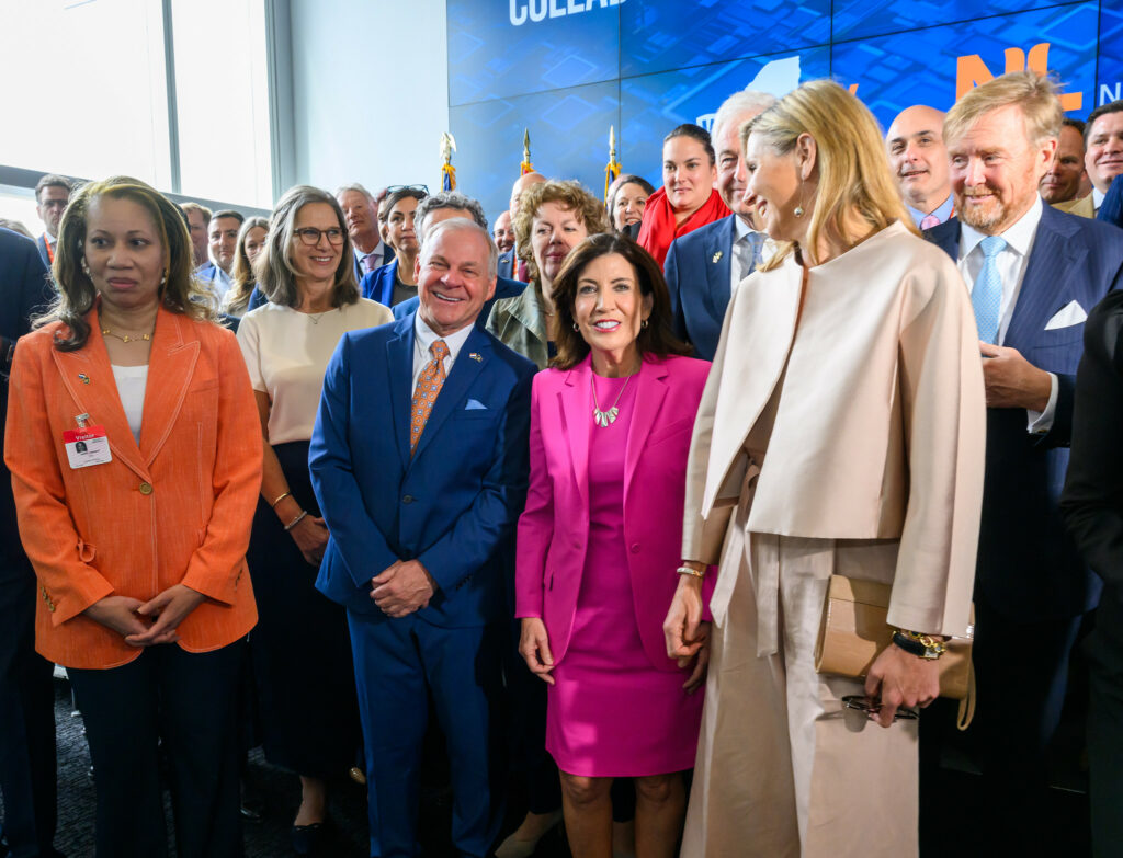
“This partnership with our Dutch counterparts will help to take New York’s chips transformation to the next level,” Governor Hochul said. “New York and the Netherlands share a belief that the countries that lead the semiconductor renaissance will chart the path forward for the rest of the world. With this MOU, we are doubling down on our commitment to putting collaboration, innovation, and sustainability front and center in our effort to build the next generation of semiconductor technology and create high-tech, good-paying jobs.”
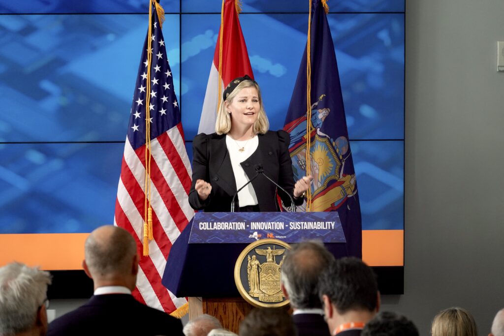
Netherlands Minister for Foreign Trade and Development Cooperation Liesje Schreinemacher said, “As leaders in semiconductor and integrated photonics development, New York State and the Netherlands are home to some of the most innovative companies, engineers, and researchers in the world. Of course we are very proud of this achievement, and, at the same time, there remains room for growth. As friends and allies, our countries can work together and pave the way for new business opportunities, greater innovation, and increased job opportunities, ultimately leading to a healthier, more prosperous and more sustainable society.”
The MOU, which was signed during the New York/Netherlands Semicon Forum at NY CREATES’ Albany NanoTech Complex, will allow for the exchange of best practices between New York and the Netherlands to drive innovative and sustainable solutions in semiconductor R&D and manufacturing. These might include innovative measures to bolster the semiconductor supply chain, as well as making strides to maximize power efficiency, water efficiency, and the development of new materials.
This new partnership also unlocks opportunities for academic collaboration between New York and Dutch universities, including a new New York State program to sponsor up to five SUNY students’ attendance at the Eindhoven Semiconductor Summer School at the Technical University of Eindhoven in the Netherlands, 5-day intensive program for STEM Masters students led by leading Dutch academic and industrial partnerships.
The announcement follows the New York/Netherlands Semicon Forum at NY CREATES’ Albany NanoTech Complex, which convened more than 100 semiconductor businesses, research and development centers, higher education institutions, policymakers, and ecosystem partners from the Netherlands and New York State to discuss how the two can cooperate to build strong, resilient, and sustainable supply chains. Sessions were held on key topics, including workforce development, environmental sustainability, and international collaboration.
“We are doubling down on our commitment to putting collaboration, innovation, and sustainability front and center in our effort to build the next generation of semiconductor technology and create high-tech, good-paying jobs.”
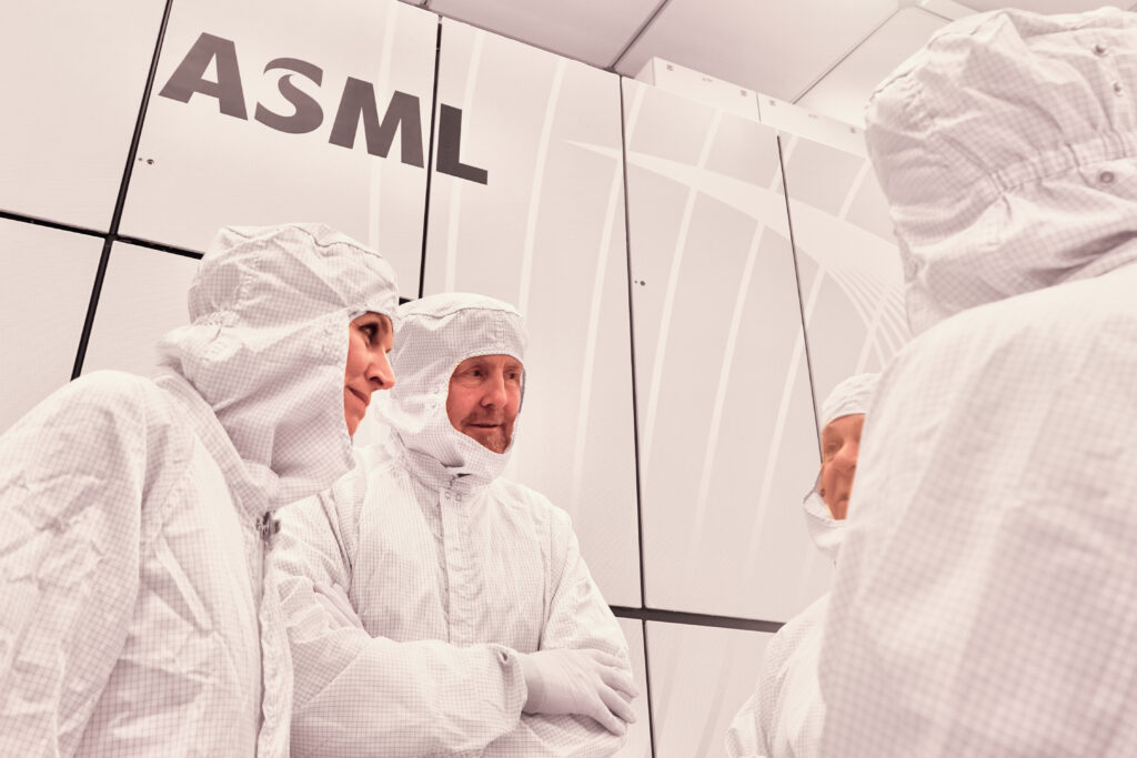
President of NY CREATES Dave Anderson said, “On behalf of NY CREATES, I am honored to host Their Majesties, the King and Queen of the Netherlands, today at our Albany NanoTechComplex, the largest and most advanced non-profit semiconductor R&D facility in North America to showcase New York State’s growing innovation ecosystem enabled by Governor Hochul’s strategic investments. Our 20-year partnership with Dutch companies ASM and ASML has been marked by incredible technological accomplishments and impactful collaborations, and I am enthusiastic about our collective journey while we continue to foster innovation and develop the next generation of semiconductor technologies together.”

Empire State Development President, CEO and Commissioner Hope Knight said, “New York State is home to some of the world’s top companies and most dynamic innovators from around the globe, and we are excited to further strengthen our strategic partnership with the Netherlands. Together, through this agreement, we will grow cutting edge businesses – especially in the semiconductor industry – and open the door to new ideas, research and talent that will create a world of opportunities.”
Governor’s Office of Semiconductor Expansion, Management, and Integration SVP & Executive Director Merideth Andreucci said, “It was an honor to participate in the New York/Netherlands Semicon Forum, and this partnership between the Netherlands and New York State will strengthen innovation and collaboration in the semiconductor industry. Today’s discussions and event exemplify our commitment to knowledge sharing, learning and adopting best practices in sustainable manufacturing with our Dutch partners.”
Governor Hochul’s Innovation Agenda
The partnership builds on Governor Hochul’s commitment to driving innovation across New York State to attract major employers and create good-paying, 21st century jobs. As part of her FY25 Enacted Budget, the Governor secured a $275 million investment in Empire AI, a consortium of seven founding institutions that will create and launch a state-of-the-art artificial intelligence computing center in Buffalo that will put New York State at the cutting-edge of AI research.
Governor Hochul also signed New York’s historic Green CHIPS legislation to drive semiconductor research, development, and manufacturing in New York State and announced a $10 billion partnership to bring next-generation chips research to NY CREATES’ Albany NanoTech Complex. By leveraging federal CHIPS and Science Act incentive opportunities with state funding, the Governor’s initiatives have unlocked historic investments from the semiconductor industry, including a $100 billion investment from Micron to build a world-class chipmaking facility and create 50,000 jobs in Central New York, as well as investments from GlobalFoundries, IBM, TTM Technologies, and other semiconductor and supply chain businesses.
In addition, the Governor has continued to advance a $620 million Life Science Initiative to support innovation in biomedical research. And through strategic investments like the $113.7 million Battery-NY initiative, Governor Hochul has fueled the growth of the sustainability, green technology, and energy storage economies in New York State.
The Governor’s innovation agenda has catalyzed major public and private investments, transforming New York’s economy and creating good-paying jobs of the future. GlobalFoundriesrecently announced an $11.6 billion investment to expand its chip manufacturing campus in New York’s Capital Region, creating 1,500 direct jobs and thousands of indirect jobs. In 2022, Micron announced a 20-year, $100 billion investment to create a megafab campus in Central New York, creating 50,000 new direct and indirect jobs and unlocking hundreds of millions of dollars in community benefits. The Governor’s Life Science Initiative helped to solidify New York’s selection for the $300 million Chan Zuckerberg Biohub New York, a biomedical research hub in New York City, and significant investments from Schrödinger, Inc., Deerfield Discovery and Development, and other life sciences businesses. Earlier this year, the National Science Foundation also announced a $160 million investment in Binghamton University’s New Energy New York Storage Engine to establish a hub for innovation, technology translation, and workforce development to grow the capacity of the domestic battery industry.
News Coverage
WAMC: Dutch royals to renew ties with visit to Albany
WYNT/NewsChannel 13: Netherlands king, queen visit nanotech campus in Albany for new partnership
Times Union: Albany’s Dutch connections get a royal look
CBS6 News: Royal family tours Albany’s NY CREATES, ignites US-Netherlands semiconductor pact
Spectrum News: Hochul and Dutch minister announce high-tech partnership during king, queen visit
News10 ABC: Dutch King and Queen visit Albany
Erie News Now: Albany receives a royal visit from the Netherlands
NY Times: A Royal Visit to the City That Was Once Called New Amsterdam (paywall)
Saratogian: Hochul, Netherlands Foreign Trade minister announce semiconductor partnership (paywall)
Times Union: After 400 years, Dutch still bringing innovation to Albany

