News Release: Fraunhofer IPMS and NY CREATES Strengthen Cooperation

Fraunhofer IPMS and NY CREATES strengthen cooperation

German-American collaboration between research institutes

Bridges of Innovation: Fraunhofer IPMS and NY CREATES strengthen cooperation

The research institutes Fraunhofer IPMS and NY CREATES provide the framework for international understanding and collaboration.

The New York Center for Research, Economic Advancement, Technology, Engineering, and Science (NY CREATES) is one of the world’s leading research and development institutions for digital technologies and microelectronics. Last year, representatives from Fraunhofer Institute for Photonic Microsystems (IPMS) met with counterparts at NY CREATES’ Albany NanoTech Complex in New York State. There, Wenke Weinreich, Deputy Director of the Fraunhofer IPMS, signed a Memorandum of Understanding in the presence of Saxony’s Minister President Michael Kretschmer.

The collaboration includes the initiation of joint research projects, symposia, and workshops, as well as the promotion of scientific exchanges. This step marks a significant milestone in the international cooperation between the two institutions, which are focused on promoting innovation and progress in the fields of digital technologies, energy technologies, and microelectronics.

“With our expertise and technologies in advanced microelectronics, we ideally complement the capabilities of NY CREATES. Together we can make significant progress in the development of future semiconductor systems,” said Dr. Wenke Weinreich.

“We are pleased to partner with Fraunhofer IPMS to pursue common goals, such as the ways in which we can further enable next-generation semiconductor research, a highly qualified workforce, and economic advancement,” said NY CREATES President Dave Anderson. “As we anticipate large-scale growth at our Albany NanoTech Complex site, including the new High NA EUV Lithography Center, we look forward to complementary collaborations with Fraunhofer IPMS along with other leading global organizations.”

NY CREATES representatives recently visited the Fraunhofer Institute in Dresden and the Silicon Saxony office where Fraunhofer IPMS and NY CREATES agreed on concrete dates for a joint exchange in 2024.

View a video featuring Dr. Weinreich, “Why Partnerships are Critical for Semiconductor Organizations,“ here.

—-

About Fraunhofer IPMS

Fraunhofer IPMS is one of the leading international research and development service providers for electronic and photonic microsystems in the application fields of intelligent industrial solutions and manufacturing, medical technology and health, and mobility. In two state-of-the-art clean rooms and with a total of four development sites in Dresden, Cottbus and Erfurt, the institute develops innovative MEMS components and microelectronic devices on 200 mm and 300 mm wafers. Services range from consulting and process development to pilot production.

About NY CREATES

NY CREATES serves as New York’s bridge to the advanced electronics industry. As the primary resource for fostering public-private and academic partnerships in New York State, NY CREATES attracts and leads industry-connected innovation and commercialization projects that secure significant investment, advance R&D in emerging technologies, and generate the jobs of tomorrow. NY CREATES runs some of the most advanced facilities in the world, boasts more than 2,700 industry experts and faculty, and manages public and private investments of more than $20 billion – placing it at the global epicenter of high-tech innovation and commercialization. Learn more at www.ny-creates.org

Contact:
Fraunhofer Institute for Photonic Microsystems (IPMS):
Frank Balvin | +49 351-8823-1144 | franka.balvin@ipms.fraunhofer.de

NY CREATES:
Steve Ference | +1 518 424-6029 | sference2@ny-creates.org

View Additional Coverage:

Azo Optics: Bridges of Innovation: Fraunhofer IPMS and NY CREATES Strengthen Cooperation

Capitol Pressroom: NY CREATES Pres. Dave Anderson, Empire State Development’s Kevin Younis Discuss New High NA EUV Lithography Center

Capitol Pressroom: NY CREATES Pres. Dave Anderson, Empire State Development’s Kevin Younis Discuss New High NA EUV Lithography Center

Capitol Pressroom

“Our guests are David Anderson, President of NY CREATES and Kevin Younis, Chief Operating Officer and Executive Deputy Commissioner of Empire State Development…We discuss Gov. Kathy Hochul’s December announcement of a public-private partnership at NY CREATES’ Albany NanoTech site, where the state is investing $1 billion on research and development equipment that will be used by Micron, IBM, and other high-tech players.”

Listen Here

NY CREATES President Dave Anderson Statement on Natcast CEO Selection

NY CREATES President Dave Anderson Statement on Natcast CEO Selection

“On behalf of NY CREATES, I congratulate Deirdre Hanford as the first Chief Executive Officer for Natcast. Her extensive background in the semiconductor design community will undoubtedly and adeptly lead this critical U.S. effort toward successful outcomes that will bolster the U.S. semiconductor ecosystem and our national security at a time when the world faces numerous technological challenges. We look forward to working with her and the Natcast board to boost high-tech R&D and manufacturing in the U.S. while simultaneously creating new jobs and economic growth. We, at NY CREATES, applaud this selection by the Natcast board and stand ready to leverage our globally recognized Albany NanoTech Complex, cutting-edge semiconductor R&D capabilities, and international partnerships with leading members of industry and academia to serve the U.S. and further strengthen our collective innovation-based competitiveness.”

-Dave Anderson
NY CREATES President

Find a link to the announcement here: https://natcast.org/deirdre-hanford-appointed-as-ceo-of-natcast

Team Including NY CREATES and Led by Jefferson Lab Tasked by DOE to Advance Superconducting Computer Chip Technology

Team including NY CREATES and led by Jefferson Lab Tasked by DOE to advance superconducting computer chip technology

NEWPORT NEWS, VA – Superconducting technologies are the lifeblood of the U.S. Department of Energy’s Thomas Jefferson National Accelerator Facility in its ongoing mission to probe the quarks and gluons inhabiting the quantum universe.

Superconducting radiofrequency (SRF) technology, a core competency of Jefferson Lab, is used to accelerate the fundamental electron particles in the lab’s Continuous Electron Beam Accelerator Facility, enabling researchers from around the world to conduct cutting-edge experiments to study the fundamental building blocks of matter. With the investment from DOE’s Office of Nuclear Physics, Jefferson Lab scientists and engineers have been constantly improving the SRF technology to benefit particle accelerators for nuclear physics and other programs in the DOE’s Office of Science. That includes innovative superconducting materials and structures.

Now, leveraging its nearly four decades of expertise and capabilities in SRF science and technology, the lab is leading a multidisciplinary team to explore concepts to use these new superconducting materials and structures in ultra-energy-efficient Superconducting Digital (SCD) electronics aimed at emerging artificial intelligence and quantum computing technologies.

The team includes imec and the New York Center for Research, Economic Advancement, Technology, Engineering, and Science (NY CREATES) — both leading hubs for high-technology research and innovation — and Cornell University. Its strength lies in bringing together concept and design (imec), fundamental material development (Jefferson Lab), characterization (Cornell), and process development and implementation (imec and NY CREATES).

Their project, “Advanced superconducting integration process enabling sustainable hardware for AI and quantum computing,” is one of 11 multidisciplinary peer-reviewed projects selected by DOE to receive a total of $73 million in investments to accelerate new technologies from discovery to commercialization. The project is being funded through the Accelerate initiative through DOE’s Offices of Advanced Scientific Computing Research and Nuclear Physics.

During the DOE review process, the collaboration was qualified as “an A+ Team … of exceptional talent.”

“Society needs faster, better-performing computer technology,” said Anne-Marie Valente-Feliciano, Jefferson Lab senior physicist and SRF process and materials group leader. “The project is aimed at developing a new computer chip technology using superconducting materials for faster performance and improved efficiency.”

From imec, Anna Herr and Quentin Herr are renowned world experts who have pioneered several new technologies for computer memory. Both are former Northrop Grumman Fellows and now scientific directors at their company. Both imec and NY CREATES are able to turn innovation into processes and device structures that will lead to faster circuits.

“Without greater innovation in high-performance computing,” said Quentin Herr, “it’s predicted that by 2040, half of the world’s energy will go toward computing.”

“In order to satisfy humanity’s need for computing, new paradigms are required,” said team member Satyavolu Papa Rao, materials scientist, engineer and vice president for research at NY CREATES. “Superconducting digital logic circuitry is a very critical path that needs to be explored, and that’s what we are doing.”

The vision is in sight

Identifying a key technology gap that currently hinders advancing digital superconductor electronics, the team’s approach is to innovate major changes, including scalability, to the existing fabrication process.

A critical goal is to develop improved superconducting and barrier materials that would perform better and tolerate higher processing temperatures, making them fully compatible with the fabrication processes of conventional electronics technology.

In a large-scale application such as AI running in a data center, superconducting materials offer a 100X improved energy efficiency, even after accounting for the overhead of a closed-loop cryogenic system for cooling. Superconducting digital logic chips (suitably modified) can also be placed near quantum computing chips, to control and communicate with them. That means that this technology is important for enabling both quantum and classical computing in the future.

Team member Katja Nowack, assistant professor of physics at Cornell University, has significant experience in the characterization of superconducting materials. Her toolbox of techniques enables imaging the properties of these materials so they can be better tuned to application at scale.

“My lab brings expertise in a pretty unique way to image the relevant materials and structures,” Nowack said. “We specialize in a type of magnetic imaging at low temperatures that we typically use to explore emergent phenomena in quantum materials. But it so happens that our imaging is well-suited to help develop a greater understanding of the fundamentals of the materials involved in SCD electronics. This is a critical need to advance the kind of technology we pursue in this project.”

“There’s potential for 100X improvement,” said Quentin Herr. “Ours is a very aggressive project, but one that’s extremely important because computing permeates all of our lives and continues to expand.”

Ever-faster computing would further revolutionize the promise of AI.

“AI needs large datasets and six-month-long learning cycles on energy-hungry computing systems today,” said Anna Herr. “Our proposed technology will allow energy-efficient learning much faster on real-time data closer to human rates of learning.”

Reaching that goal, however, won’t happen overnight.

“Eventually,” said Valente-Feliciano, “the materials and technology are going to mature to where they can be implemented in devices useful for the community at large. Of course, this will happen in stages — you’re not going to find a computer like that on the shelf tomorrow. But you can imagine it can be used for experiments and larger data centers.

“It is exciting to see the development of such a concept using our research in innovative materials coming to reality and being used in the future by society. It will take a long time, but that is our vision.”

Accelerating innovation

DOE’s larger goal with its Accelerate initiative is to fuel innovation in basic research so that new materials and technologies can be scaled and transitioned into new products and capabilities to enhance the country’s economic health and security.

“This research will integrate novel concepts and approaches in use-inspired basic research to address gaps or challenges that limit the ultimate transition to applied research for further development and demonstration,” said Asmeret Asefaw Berhe, director of DOE’s Office of Science, in announcing the grants. “Achieving these research goals will greatly accelerate the innovation cycle, which currently can take years to decades to realize.”

The 11 funded projects are supported by the Office of Science programs in Advanced Scientific Computing Research, Biological and Environmental Research, Basic Energy Sciences, Fusion Energy Sciences, High Energy Physics, Nuclear Physics, and the DOE Isotope Program.

Each project is led by a national laboratory with partners from other national labs, industries and universities, often including Historically Black Colleges and Universities (HBCUs) and Minority-Serving Institutions (MSIs).

This project is one of several at Jefferson Lab that aims to apply the lab’s expertise in niche technologies toward innovations that will have a positive impact on society. It is supported by DOE’s Offices of Advanced Scientific Computing Research and Nuclear Physics. Learn more about opportunities for partnering with Jefferson Lab in our Technology Transfer pages.

Further Reading
Department of Energy Announces $73 Million for Basic Research to Accelerate the Transition from Discovery to Commercialization

By Tamara Dietrich

Contact: Kandice Carter, Jefferson Lab Communications Office, 757-269-7263, kcarter@jlab.org

-end-

Jefferson Science Associates, LLC, manages and operates the Thomas Jefferson National Accelerator Facility, or Jefferson Lab, for the U.S. Department of Energy’s Office of Science. JSA is a wholly owned subsidiary of the Southeastern Universities Research Association, Inc. (SURA).

DOE’s Office of Science is the single largest supporter of basic research in the physical sciences in the United States and is working to address some of the most pressing challenges of our time. For more information, visit https://energy.gov/science

Summary: A multidisciplinary team led by Jefferson Lab and including imec, NY CREATES, and Cornell University has been selected by DOE to advance a superconducting approach to advanced computer chip technology. The team will explore concepts to use new superconducting materials and structures in ultra-energy-efficient Superconducting Digital (SCD) electronics aimed at emerging artificial intelligence and quantum computing technologies.

View Original News Release

GOVERNOR HOCHUL ANNOUNCES $10 BILLION PARTNERSHIP TO BRING NEXT-GENERATION RESEARCH AND DEVELOPMENT CENTER TO NY CREATES’ ALBANY NANOTECH COMPLEX

GOVERNOR HOCHUL ANNOUNCES $10 BILLION PARTNERSHIP TO BRING NEXT-GENERATION RESEARCH AND DEVELOPMENT CENTER TO NY CREATES’ ALBANY NANOTECH COMPLEX

December 11, 2023


Albany NanoTech Will House North America’s First and Only Publicly Owned High NA Extreme Ultraviolet Lithography Center – Bringing the Future of Advanced Semiconductor Research & Manufacturing to New York’s Capital Region

Project Will Unlock Transformative Benefits Including Thousands of New Direct, Indirect, and Union Construction Jobs and Strong Commitments to Workforce Development and Sustainability 

Partnership Includes Significant Private Investment From IBM, Micron, Applied Materials, Tokyo Electron and Other Industry Leaders That Will Integrate Cutting-Edge Chipmaking Technology into Their R&D Efforts 

Builds on Governor Hochul’s Agenda to Establish a Global Hub for Semiconductor Manufacturing and Innovation Upstate

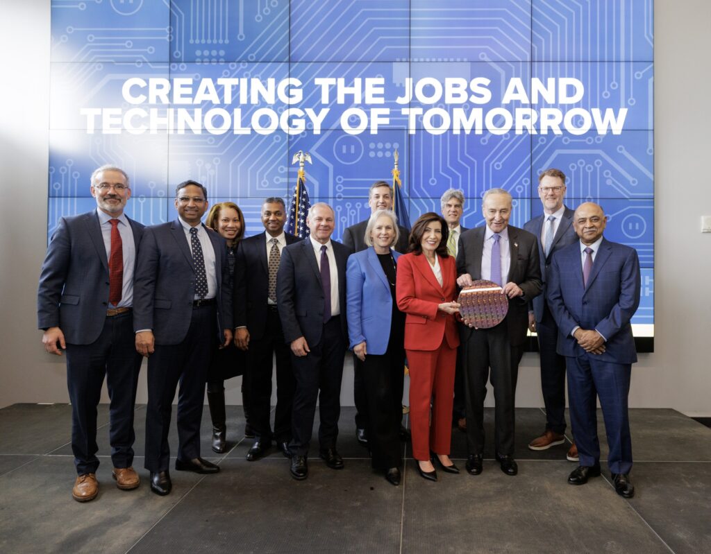
Governor Kathy Hochul today announced a $10 billion partnership with leaders from the semiconductor industry such as IBM, Micron, Applied Materials, Tokyo Electron, and others to establish a next-generation semiconductor research and development center at NY CREATES’ Albany NanoTech Complex. The partnership will fund the construction of a cutting-edge High NA Extreme Ultraviolet Lithography Center – the first and only publicly owned High NA EUV Center in North America – that will support the research and development of the world’s most complex and powerful semiconductors. In addition to the transformative investment in New York’s Capital Region, this partnership will make New York State home to the nation’s most advanced, publicly owned semiconductor R&D infrastructure, support the long-term growth of New York’s tech economy, and create and retain thousands of direct, indirect, and union construction jobs.

“This $10 billion partnership to bring innovative chips research to the Capital Region should send a message to the entire industry: New York is open for business,” Governor Hochul said. “From our Green CHIPS legislation to Micron’s historic investment and the creation of GO-SEMI, we’re building the future of semiconductor research right here in New York. This industry is creating real opportunity in our state with major regional investments, countless new jobs, and bold commitments to workforce development and sustainability, and my administration will keep working with elected and industry leaders to make New York a global chipmaking superpower.”

Under this new initiative, NY CREATES will acquire and install a High NA EUV lithography tool, designed and manufactured by ASML, at its Albany NanoTech Complex, where industry partners including Micron, IBM, Applied Materials, Tokyo Electron, and others will use the most advanced semiconductor equipment ever made. Once built, New York’s High NA EUV Center will position the state as a destination for research and development of the innovative chip technology that powers nearly every smartphone, tablet, laptop, and computer server today. The Center will also foster international partnerships as world-renowned research organizations expand their presence here, drawing businesses from around the globe.

In addition, this partnership will significantly enhance New York State’s position as a leading candidate to secure anchor hub status under the federal National Semiconductor Technology Center, a designation with the potential to unlock more than $11 billion in federal CHIPS and Science Act funding.

This project will create at least 700 new direct jobs and retain thousands of jobs, leverage at least $9 billion in private spending and investment, and establish significant commitments to support and build talent development pipelines, including through partnerships with the State University of New York. Partners have committed to either expanding or initiating support for workforce development programming, including investments in SUNY, Rensselaer Polytechnic Institute, and other public and private workforce development activities; K-12 STEM academic programs; training, internships, and experiential learning to undergraduate and graduate students in engineering and related STEM fields, and academic research partnerships.

NY CREATES and industry partners have also agreed to a range of sustainability commitments throughout the construction and operational phases of the project that are closely aligned with New York’s nation-leading Green CHIPS program, including use of best available technology for greenhouse gas emission reduction; prioritization of renewable energy, with preference for New York sources; and pursuit of minimum Gold LEED status certification for new buildings related to the project. Additionally, partners are committed to integrating sustainability as a primary goal of R&D activities, including sustainable semiconductor manufacturing processes, materials use, waste reuse and reclamation, and fab design. Through this new focus, the High NA EUV Center is positioned to become a global leader in the development of sustainable and climate-friendly semiconductor manufacturing processes and technology.

To support this project, New York State is investing $1 billion to expand the Albany NanoTech Complex with the establishment of the High NA EUV Center through the purchase of ASML’s EXE:5200 High NA EUV scanner, as well as the construction ofNanoFab Reflection, a new, highly sophisticated building with more than 50,000 sq. ft. of cleanroom space that will encourage future partner growth and support new initiatives like the National Semiconductor Technology Center, National Advanced Packaging Manufacturing Program, and Department of Defense Microelectronics Commons program, the latter of which was recently awarded to New York State. The project will create an estimated peak of 500 to 600 union construction jobs at prevailing wage during the two-year construction phase.

The project is critical to further growing NY CREATES’ Albany NanoTech Complex. In addition to creating 50,000 square feet of state-of-the-art cleanroom space at Albany NanoTech, it is anticipated that this investment opens the door to the construction of additional future cleanroom space to enable the projected long-term growth of new and existing collaborations spurred by the High-NA EUV Center and federal initiatives.

Senate Majority Leader Chuck Schumer said, “This is a landmark day for the Capital Region. With this groundbreaking $10 billion public-private partnership, spurred by my CHIPS and Science Act, industry has made it clear: the Albany NanoTech Complex is home to America’s semiconductor R&D future. This historic partnership will bring the most cutting-edge machinery in the world to Upstate NY, helping make discoveries that engineers today cannot even fathom – ensuring the U.S. leads the world in semiconductor innovation and manufacturing and bringing us closer to turning science fiction into reality by producing microchips smaller than a nanometer, right here in the Capital Region. This $10 billion means hundreds of new high-paying tech and construction jobs, along with scientists and leading companies from around the world turning to the Capital Region as the place where they conduct their research. I wrote the CHIPS & Science Act because I knew it would be transformative for Upstate New York, which was perfectly suited to bring this industry that is vital to America’s national security and economic future back from overseas. Under Governor Hochul’s leadership, New York has not only answered the call put out by the feds, but helped create a national model with unprecedented investment in every corner of Upstate NY and today’s announcement is just the latest example of how New York is leading our nation in developing the next generation of technology.”

Senator Kirsten Gillibrand said, “This investment in Albany NanoTech will reinforce New York’s position as a global leader in semiconductor research and development. This next-generation research and development center will be the only facility of its kind in the Western Hemisphere and will draw in major businesses from around the world, grow the state’s tech economy, and potentially unlock billions in federal investments to the Capital Region. Establishing this new semiconductor center will also bolster our national security, allowing the United States to develop the world’s most complex and powerful semiconductors right at home. I am proud to see this partnership come to life and look forward to continuing to work to make the Capital Region a global leader in semiconductor research and manufacturing.”

Representative Paul Tonko said, “I’ve long pushed for strong investments in our chips manufacturing to strengthen our domestic supply chains, create good-paying jobs, and lower costs for American consumers. Thanks to that effort and provisions in our CHIPS and Science Act, our Capital Region – already home to a robust network of chip manufacturers, state of the art research facilities, and educational institutions – is poised to lead the nation in this sector, driving innovation and strengthening our economy. This partnership builds upon the pioneering spirit of innovation that our region has long represented. I’m grateful to all those whose dedication is enabling further development and growth in this industry.”

IBM Chairman and CEO Arvind Krishna said, “At the New York State Albany NanoTech Complex, IBM and our partners are leading the world in semiconductor R&D advances that make chips smaller, more powerful, and more energy efficient. The new High NA EUV Center at Albany NanoTech will secure a strong pipeline for semiconductor innovation, keeping New York State at the center of semiconductor expertise, accelerating the growth of the global chip industry and helping to meet manufacturing demand for new technologies such as generative AI. IBM is proud to call New York State our home, and to support this critical investment towards new breakthroughs in semiconductor technology.”

Micron President and CEO Sanjay Mehrotra, said, “The High NA EUV Center at NY CREATES’ Albany NanoTech Complex is a critical step in advancing next-generation semiconductor R&D in America and will put New York at the forefront of future innovation and technology leadership. One of the key factors that made New York the ideal future home for our megafab was the state’s history of semiconductor development and manufacturing and the strong opportunities for R&D ecosystem collaboration that Micron can help scale with our memory technology leadership. Alongside our state and federal partners and with critical funding support from the CHIPS and Science Act, we look forward to building and training a highly skilled talent pipeline through North America’s first and only High NA EUV Center.”

Semiconductor Products Group at Applied Materials President Prabu Raja said, “We are pleased to see continued investments to strengthen the chipmaking R&D ecosystem in New York State. At our Materials Engineering Technology Accelerator (META Center) at Albany NanoTech, Applied is collaborating with customers to pioneer new semiconductor materials, structures and devices for improving chip performance and energy efficiency. Expanding the footprint and capabilities of the NanoTech campus will build upon our longstanding partnership with New York State and provide another avenue to accelerate the time from concept to commercialization of next-generation chipmaking technologies.”

Tokyo Electron (TEL) President and CEO Tony Kawai said, “We are looking forward to continuing our decades-long partnership with New York State through the opening of the new R&D center at the Albany NanoTech Complex. High NA EUV is the semiconductor industry’s most advanced manufacturing technology, and TEL is excited to contribute to the development of the global semiconductor industry and the innovation in this space that this new development will spur.”

ASML President and CEO Peter Wennink said, “We are proud that ASML tools enable our customers to produce the chips the world needs. This significant investment by New York in cutting-edge High NA EUV technology will fuel innovation in our ecosystem and accelerate chipmakers’ ability to manufacture tomorrow’s more advanced chips faster and more cost-effectively.”

Establishing a Global Semiconductor Hub in New York State
Governor Hochul has maintained a strong commitment to building a modern economy in New York State by growing the semiconductor industry and attracting innovative businesses that create good paying, 21st century jobs. In October 2022, after signing New York’s first-in-the-nation Green CHIPS legislation to build a thriving, sustainable chips industry, the Governor announced an historic $100 billion investment from Micron to establish a state-of-the-art leading-edge memory manufacturing campus in Central New York that will create 50,000 jobs. Since signing Green CHIPS, the Governor has also announced major investments from several other semiconductor manufacturers and companies from the semiconductor supply chain, including AMD, Edwards Vacuum, and TTM Technologies to expand their presence in New York.

In her 2023 State of the State address, Governor Hochul announced the creation of the $45 million Governor’s Office of Semiconductor Expansion, Manufacturing, and Integration, known as GO-SEMI, to oversee the state’s efforts to continue to grow the industry.

New York’s Albany NanoTech Complex
The Albany NanoTech Complex, owned and operated by the non-profit New York Center for Research, Economic Advancement, Technology, Engineering, and Science, or NY CREATES, is the most advanced, publicly-owned 300 mm semiconductor R&D facility in North America and has been at the forefront of semiconductor innovation for more than two decades. The site currently houses the current generation of EUV lithography equipment, which IBM recently used to produce the world’s first 2 nanometer chip technology – the smallest scale ever developed. The High NA EUV Center will bring the next generation of EUV equipment to Albany NanoTech and firmly establish New York as the epicenter of leading-edge semiconductor R&D.

Empire State Development President, CEO and Commissioner Hope Knight said, “New York State has invested billions of dollars over the last several years to make Albany NanoTech the most advanced publicly owned semiconductor research and development center in North America and this is the next step in its evolution. This investment will literally catapult New York State to the forefront of semiconductor R&D and continue our efforts to make New York State the semiconductor capital of the nation. We are also ensuring that sustainability and workforce development opportunities are a priority so that the next generation of New Yorkers are well placed for opportunities in this industry.”

NY CREATES President Dave Anderson said, “Governor Hochul’s vision to make New York State the epicenter for semiconductor-based R&D is undoubtedly coming to fruition as a result of today’s historic investment by New York and our industry partners. This funding will support construction of the new NanoFab Reflection building at NY CREATES’ Albany NanoTech Complex to house the world’s most advanced, next-generation extreme ultraviolet lithography equipment. As a result of this historic investment, under the leadership of Governor Hochul and the continued and tireless support from Senate Majority Leader Schumer, NY CREATES and our partners will secure our place at the forefront of global chip development for years to come. This expansion sets the stage for long-term growth and new job opportunities here and throughout the state, contributing significantly to the nation’s innovation economy and demonstrating why the Albany NanoTech Complex is ready to host the critically important National Semiconductor Technology Center.”

Imec President and CEO Luc Van den hove said, “Imec is pleased to support the High NA EUV Center to be set up at the Albany NanoTech Complex. This initiative will speed up the industrial adoption of the most advanced semiconductor manufacturing technology in the U.S. The introduction of High NA EUV needs radical innovations on the process side. To anticipate this in a proactive way, imec has set up a joint high-NA EUV lab with ASML, built around the very first high-NA scanner. Working closely with the global patterning ecosystem, we are preparing the process innovations and de-risking the technology. and we are eager to work with the partners at NY CREATES on this complementary strategic effort to push the boundaries of chip scaling and performance.”

View original news release here; view a transcript of the announcement event, video, and photos here.

News Coverage

New York Times: New York Plans to Invest $1 Billion to Expand Chip Research
Wall Street Journal: New York Joins IBM, Micron in $10 Billion Chip Research Complex
New York Post: New York state teaming up with IBM, Micron to invest in $10 billion chip research complex
Times Union: IBM, Micron to headline $10 billion chip research program in Albany
Syracuse Post-Standard: $10 billion cutting-edge semiconductor research center coming to Albany
Albany Business Review: New York, chip firms to invest $10B at Albany NanoTech
CBS6: Landmark $10 billion investment to boost research at Albany NanoTech
Spectrum News: Hochul: $10 billion going to semiconductor research, development center at Albany NanoTech Complex
WTEN: $10 Billion semiconductor infrastructure coming to Albany
WNYT: Huge partnership expected to help put Albany at forefront of nanotech
WAMC: New York Gov. Kathy Hochul announces $10 billion partnership at Albany NanoTech Complex
CNN: New York plans a $10 billion chip research center with IBM, Micron and others
Daily Gazette: Hochul: State, tech industry to collaborate on Albany chip research center
$10B Earmarked for Development of Extreme-UV Lithography Center | Business | Dec 2023 | Photonics Spectra
Micron’s local work will benefit from research investment and really big machine in Albany (localsyr.com)

‘NY CREATES president: Albany primed for semiconductor growth’ – Albany Business Review

'NY CREATES president: Albany primed for semiconductor growth' - Albany Business Review

‘NY CREATES president: Albany primed for semiconductor growth’ – Albany Business Review

Albany Business Review

“What potential do you see in Albany as a player in the semiconductor industry?

“The capabilities that we have here are the most advanced we have in the
country today. But the potential for going even further is enormous
today because of the CHIPS Act, because of the new applications and the
technologies that will drive them. We have the capabilities to help a
broad spectrum of industry partners get to where they want to go from a
research standpoint, and engaging with the SUNY system and the
universities always drives new technologies. And so our capabilities are
fantastic. Our expansion and potential for expansion into the future is
going to be right in line with the industry growth.”

View the article

The Capitol Pressroom: NY CREATES Hopes to Steer State’s High-Tech Future

The Capital Pressroom Coverage Article - Cleanroom Image

In a wide-ranging conversation, NY CREATES President Dave Anderson spoke with The Capitol Pressroom host David Lombardo about NY CREATES and what the organization does to support New York State–and the nation’s—technological progress, and more. Listen here.

NY CREATES AND PSIQUANTUM JOIN FORCES FOR INTEGRATED PHOTONICS RESEARCH AND DEVELOPMENT PARTNERSHIP

NY CREATES AND PSIQUANTUM JOIN FORCES FOR INTEGRATED PHOTONICS RESEARCH AND DEVELOPMENT PARTNERSHIP

Industry demand for integrated photonics has historically been driven by the need for higher-performance networking, especially in telecom and datacenter applications. More recently, the technology has seen a surge of interest in the context of high-performance computing systems for training and running large-scale machine learning models. It also has wider applications, including imaging, sensing, and optical accelerators for computing.

Integrated photonics technology uses standard semiconductor manufacturing processes to fabricate chips containing microscopic optical elements, such as waveguides, beam-splitters, lasers, and detectors. PsiQuantum is developing a large-scale photonic quantum computer in which these components are repurposed to generate and manipulate single photons – particles of light – which are then used to encode quantum information. Several other quantum computing efforts are also beginning to integrate photonic devices into their systems, as they seek to scale from proof-of-principle single-chip systems toward utility-scale, error-corrected quantum computers.

PsiQuantum’s strategy aims to accelerate the path to the considerable volume, yield, and performance required for very large, impactful quantum computers by leveraging the standard manufacturing processes, tools, and materials of the semiconductor industry.

Now, a new partnership between the New York Center for Research, Economic Advancement, Technology, Engineering, and Science (NY CREATES) and PsiQuantum is expected to open new avenues for technological advancements, facilitating the development of these quantum technology solutions that can have far-reaching implications. By leveraging each organization’s respective expertise and resources, NY CREATES and PsiQuantum aim to significantly advance the integrated photonics landscape with far-reaching applications in quantum computing, telecommunications, and many more.

NY CREATES’ Albany NanoTech Complex is the largest and most advanced, public/private 300mm semiconductor R&D center in North America, and it includes state-of-the-art tools within a flexible research environment that supports rapid learning cycles – all of which will enable PsiQuantum, through this collaboration, to accelerate its technical roadmap to deliver the world’s first large-scale, error-corrected quantum computer.

One of the first activities of the partnership focuses on integrating ultra low-loss waveguides with Barium Titanate (BTO), a pioneering ultra-high performance optical material. Practically, this involves precisely bonding wafers of silicon photonics, such as those being built by PsiQuantum in New York, on top of wafers of BTO, produced in PsiQuantum’s facility in San Jose, California.

“This collaboration between NY CREATES and PsiQuantum marks a critical step forward in the development of quantum switching circuits,” said David Anderson, President of NY CREATES. “By combining our collective expertise and the world-class capabilities available at our Albany NanoTech Complex, we are poised to push the boundaries of what is possible in the field of quantum technology. We are excited about the potential impact this partnership can have on industries such as telecommunications, where advanced switching capabilities are in high demand.”

“We are thrilled to partner with NY CREATES on this groundbreaking research and development endeavor,” said Fariba Danesh, Chief Operating Office at PsiQuantum. “This unique joint-development research environment has enabled us to access cutting-edge tools, accelerate our learning cycles, and drive innovation at an unprecedented pace. Our collaboration represents a significant opportunity to develop switching circuits with the potential to outperform existing technologies and integrate them into the foundry ecosystems for volume production.”


################

About NY CREATES
NY CREATES is a technology accelerator focused on driving innovation, collaboration, and economic growth. By leveraging New York State’s unique assets, including leading academic institutions, industry partners, and government agencies, NY CREATES fosters breakthrough technologies, supports startups, and facilitates partnerships to address critical challenges and drive positive societal impact. NY CREATES oversees some of the most advanced facilities in the world, boasts more than 2,700 industry experts and faculty, and manages public and private investments of more than $20 billion – placing it at the global epicenter of high-tech innovation and commercialization. Learn more at www.ny-creates.org. 

About PsiQuantum
Powered by breakthroughs in silicon photonics and fault-tolerant quantum architecture, PsiQuantum is building the first utility-scale quantum computer to solve some of the world’s most important challenges. PsiQuantum’s approach is based on single-photon qubits, which have significant advantages at the scale required to deliver a fault-tolerant, general-purpose quantum computer. With photonic chips manufactured in world-leading semiconductor fabs, PsiQuantum is uniquely positioned to deliver quantum capabilities reaching the scale needed to drive advances in climate technologies, pharmaceuticals, healthcare, finance, energy, agriculture, transportation, communications and beyond. To learn more, visit www.psiquantum.com.

###

Contact:
NY CREATES Contact: Steve Ference | (518) 424-6029 | sference2@ny-creates.org
PsiQuantum Contact: Caleb Randall-Bodman |
media@psiquantum.com

News Release: SCHUMER SECURES COMMITMENT FROM SOUTH KOREA PRESIDENT YOON FOR KOREA TO PARTNER WITH NY CREATES’ ALBANY NANOTECH COMPLEX FOR ADVANCED SEMICONDUCTOR RESEARCH & DEVELOPMENT

While Leading A Bipartisan Congressional Delegation In Asia Earlier This Week, Schumer – Always With Upstate NY On His Mind – Met With The Korean President & Urged Korea To Expand Their Research At NY CREATES’ Albany NanoTech Complex – Which They Agreed To Do

New Commitment Will Help Expand Advanced Chip R&D And Student & Faculty Exchanges With The Republic Of Korea; Schumer Says Global Recognition Strengthens Capital Region Even Further To Become Major Hub For The National Semiconductor Technology Center

Schumer: NY CREATES’ Groundbreaking Research At The Albany NanoTech Complex Is Recognized Around The Globe, And Now Korea Will Join NY In Helping Make New Discoveries For The Future Of Chip Research

U.S. Senate Majority Leader Chuck Schumer, in a personal meeting in Seoul with South Korean President Yoon Suk Yeol earlier this week, secured a commitment that the Republic of Korea will partner with the New York Center for Research, Economic Advancement, Technology, Engineering, and Science (NY CREATES) on advanced semiconductor technology research & development at the Albany NanoTech Complex. This builds on the joint declaration signed earlier this year to promote collaboration and partnership between NY CREATES and the Korea Institute for Advancement of Technology (KIAT). Schumer said this new international collaboration with the Republic of Korea will further propel NY CREATES’ Albany NanoTech Complex as a premier global center for semiconductor research, and strengthen the facility as an ideal major hub for the National Semiconductor Technology Center (NSTC) that was established in the CHIPS & Science Act.

“Even halfway across the globe in South Korea, I always have the Capital Region and Upstate NY on my mind. During my meeting with South Korean President Yoon, I raised how important it was for our countries to work together on advanced technologies from semiconductors to AI, so our scientists and students could learn from each other to help spur innovation and take us to the next frontier,” said Senator Schumer. “I am proud to say that President Yoon agreed, and personally committed to growing South Korea’s partnerships with New York on research & development for semiconductors and other advanced technologies, including a collaboration with NY CREATES at its Albany NanoTech Complex. This will help bring researchers, Korean universities and companies to the Albany NanoTech Complex’s world-renowned facilities. Governments and industry partners from around the world continue to recognize that Albany NanoTech is the place to be for cutting-edge semiconductor research. In fact, President Yoon made clear that the U.S. and Korea working together on advanced technology is key to the alliance between our two countries, and that New York is central to that effort.”

“This partnership with the Korea Institute for Advancement of Technology is the latest step in our mission to make New York State a chipmaking superpower,” Governor Hochul said. “Research institutions like Albany NanoTech are the engines behind our state’s drive to attract, expand, and innovate the semiconductor industry, and with steady state support and the Majority Leader’s continued advocacy, we will keep tapping the best minds from New York and abroad to build our competitive edge in this sector and plan the future of chip manufacturing in our state.”

“We are grateful for Senator Schumer’s steadfast efforts and President Yoon’s commitment for Korea to partner with NY CREATES for semiconductor-based R&D. Meaningful international collaborations with our allies are important for developing critical next-gen technologies and further establishing NY CREATES and Upstate New York as an international hub for innovation-centered partnerships by leveraging our world-class resources and facilities, high-tech expertise, and workforce development initiatives,” said NY CREATES President Dave Anderson. “We are excited about the opportunities to collaborate with global tech leaders, and we look forward to finding ways to bolster domestic research and production capabilities right here in New York and the U.S., while also supporting our partners around the world.”

The direct commitment Schumer was able to secure in Korea will build on months of ongoing conversations between the Republic of Korea and NY CREATES to expand R&D, academic research, and student & faculty exchanges. Earlier this year, NY CREATES and the Korea Institute for Advancement of Technology (KIAT) signed a joint declaration to promote collaboration and partnership between the two organizations in the field of technological innovation, with a primary focus on semiconductors. The agreement was signed in Washington, D.C., during the official state visit of President Yoon. At the signing ceremony, NY CREATES President David Anderson and KIAT President Byung-joo Min were joined by U.S. Secretary of Commerce Gina Raimondo and Republic of Korea Minister of Technology, Industry, and Energy Lee Chang Yang. The agreement between NY CREATES and KIAT promotes cooperation in innovation, education, and workforce development between companies and educational institutions from Korea and New York. NY CREATES will support the U.S. component of the collaboration by providing access to its world-leading facilities for R&D and prototyping – the Albany NanoTech Complex – as well as scientists and researchers. Since this initial agreement was struck, efforts have been underway to formalize Korean support for the partnership, including putting in place specific programs and Korean investment. President Yoon’s commitment to Schumer now solidifies a path forward to finalizing that partnership.

Schumer has fought tirelessly to lift up the Capital Region and Upstate New York as a major hub to lead the nation in semiconductor manufacturing and research. Most recently, Schumer announced that following his push, NORDTECH, a New York-based consortium led by NY CREATES in partnership with Cornell, RPI, the University at Albany CNSE, and IBM, was one of the first major recipients of funding through his CHIPS & Science Act, securing $40 million through the Department of Defense’s (DoD) Microelectronic Commons Program. Earlier this year, Schumer also personally invited NY CREATES head Dave Anderson to President Biden’s 2023 State of the Union address to highlight his push to land the NSTC in the Capital Region. Prior to the passage of the CHIPS & Science Act, Schumer not only brought the Commerce Secretary to Malta to highlight opportunities for expansion at GlobalFoundries and across Upstate New York’s semiconductor industry, but also arranged for Secretary Raimondo to meet with NY CREATES and industry leaders, including from IBM and Applied Materials, to discuss the unique assets the region has for leading the NSTC.  Schumer also brought Commerce Deputy Secretary Don Graves to Albany to tour the Albany NanoTech Complex and see firsthand how the Capital Region is perfectly suited to stand up the NSTC and begin boosting the nation’s semiconductor industry.

View original news release

                                                                      ###

Read News Coverage from the Times Union here.