FuzeHub Blog: Quantum Computing: What Manufacturers Need to Know

Photo courtesy of FuzeHub

Quantum computing is an emerging technology that excites computer scientists and confounds manufacturers. It seems abstract, theoretical, and far-removed from the realities of production, logistics, and materials engineering. Yet quantum computing isn’t science fiction. This early and evolving discipline will eventually reshape industries that depend on process optimization, physical simulation, and complex decision-making.

This article distills an in-depth interview with Dr. Satyavolu “Pops” Papa Rao, Senior Director of Emerging Technologies and Research at NY Creates in Albany, New York. Pops holds a Ph.D. in Materials Science & Engineering from the Massachusetts Institute of Technology and leads work on fabrication of quantum devices at NY Creates, a non-profit organization that owns and operates the Albany NanoTech Complex – North America’s largest, most advanced public-private semiconductor research R&D facility, conducting R&D in areas ranging from semiconductors, quantum technologies, advanced memory, integrated photonics, devices for neuromorphic computing and AI, advanced packaging and Heterogeneous Integration (HI), and more.

The goals for this article are simple: explain what quantum computing is, why it matters, and where it might realistically impact manufacturing in the coming decade. FuzeHub would like to thank Pops for making this possible.

What Makes Quantum Computing Different?

To understand quantum computing, it helps to start with how today’s computers work. Classical computers, as they’re known, use transistors to process data as binary digits (bits). In turn, each bit is set to either 0 (off) or 1 (on) to align with the physical, two-state nature of electronic hardware. From CNC controllers to shop floor PCs, today’s digital devices depend on this binary system.

Quantum computers use quantum bits (qubits) instead. Unlike classical bits, qubits can exist in multiple states. In other words, qubits can exist not just as 0s or 1s, but also as a mixture of both. “A coin toss provides an analogy,” Pops says. A coin lying flat is like a classical bit with heads (0) on one side and or tails (1) on the other. A coin spinning in the air is temporarily both heads and tails.

That’s also a good way to visualize superposition, a principle of quantum mechanics that describes how subatomic particles like electrons can exist in multiple states or locations simultaneously. Quantum computers also use quantum entanglement, a phenomenon where two qubits become linked so tightly that changing one instantly affects the other, regardless of space. “These two qubits are joined together as one entangled object.” Pops explains, “even if they’re far apart.”

Why is Quantum Computing a Breakthrough?

Superposition and entanglement give quantum computing its power and access to much greater computational capabilities. That’s why these computers have the potential to solve certain problems far more quickly than classical systems. Yet quantum computing isn’t “faster” in the traditional sense. Rather, it’s a fundamentally different way of processing information that still involves algorithms: sequences of rules or instructions for solving a problem or completing a task.

Quantum computing’s most famous algorithm is Shor’s algorithm, which can factor very large numbers exponentially faster than classical computers. Shor’s algorithm matters because today’s encryption techniques depend on how classical computers would need millions of years to crack the encryption. Other quantum algorithms offer polynomial speedups, computational improvements with potential applications such as logistics resource and financial portfolio risk optimization or the modeling of physical processes.

Quantum Computing Today: Real Machines, Real Progress

Quantum computing is not hypothetical. In fact, there’s a machine in the Capital Region. Rensselaer Polytechnic Institute (RPI) in Troy, New York, has an IBM Q System One. IBM debuted the world’s first integrated quantum system for commercial and scientific use at the CES Show back in 2019. But that doesn’t mean this technology is ready to solve the thorniest problems facing small-to-medium manufacturers.

“It’s been said that people always underestimate the impact of technology in the long term and overestimate it over the near term,” Pops notes. Today, IBM is joined by Google, and a host of smaller players and startups who are advancing competing quantum technologies. There isn’t a clear winner yet, but the impact in the next decade or two could be profound. Just as silicon carbide (SiC) was once a niche research topic, SiC semiconductors now power electric vehicles and LED lighting.

Where Quantum Computing Could Impact Manufacturing

There are four principal areas where quantum computing could eventually improve manufacturing:

  • Process optimization
  • Fluid dynamics and aerodynamics
  • Materials discovery and simulation
  • Energy efficiency

Quantum computers are well-suited to solving optimization problems because they can explore many possible solutions simultaneously. That’s why Wall Street firms are using them to explore portfolio optimization. For example, Goldman Sachs has developed and deployed quantum algorithms that could allow the firm to price financial instruments at quantum speeds. In financial markets, computing speed is a tremendous advantage.

Someday, small-to-medium manufacturers could use quantum computers to solve problems such as how to route parts, schedule production, minimize downtime, and allocate limited resources. Simulating fluid flow is another potential application. Aerospace, automotive, turbomachinery, chemical processing, and semiconductor crystal manufacturers could all benefit since even small improvements in simulation accuracy can lead to major gains in performance and efficiency.

Materials discovery and simulation may be the most transformative long-term application. Quantum computers are inherently suited to simulating things like the behavior of electrons in materials. That could accelerate the discovery of new alloys and high-performance polymers. It could also lead to stronger composites, better magnets, more efficient catalysts, and advanced battery chemistries. “You need a quantum computer in order to simulate nature,” Pops explains.

Today’s quantum computers are too small to simulate anything beyond simple molecules like water and lithium hydride, but there’s steady progress on multiple fronts. That includes reducing the energy footprint of data centers that use artificial intelligence (AI) for applications like automation and simulation. Pops cautions against the “hype” surrounding quantum computing, but he foresees advances that could help manufacturers of all sizes in the 10 years.

What Can Manufacturers Expect in the Next Decade?

There are three main areas were manufacturers can expect to see progress in the shorter-term.

  • Early quantum-inspired optimization tools that run on classical computing hardware but borrow ideas from quantum algorithms.
  • Hybrid-quantum-classical workflows where certain steps of a simulation or optimization problem are offloaded to small quantum processors.
  • Improvements in materials R&D pipelines that use quantum-enhanced simulation.

There are also three areas where major advances won’t happen in the next decade.

  • Fully quantum-driven factories
  • Large-scale materials simulation
  • Real-time quantum control of manufacturing equipment

“Those require systems that are larger and more stable than what exists today,” Pops says. “The most likely future,” he adds, “are hybrid systems that combine multiple qubit types for functions such as memory, communication, or computation.”

What Should Manufacturers Do Now?

Quantum computing isn’t ready for prime-time, but manufacturers who wait to start learning, experimenting, and preparing risk falling behind the competition. “Now is the time to build internal expertise,” Pops suggests. Practical steps include:

  • Identifying optimization problems that could benefit from quantum approaches
  • Partnering with R&D centers, universities, or national labs
  • Exploring quantum‑inspired algorithms
  • Training engineers in quantum fundamentals
  • Monitoring developments in materials simulation

Quantum computing may never replace classical computing, but examining a new tool that will eventually sit alongside today’s systems could give you an edge.

From Apprenticeship to Advancement: Quazi Ummehany’s Continued Growth at NY Creates

By the National Institute for Industry and Career Advancement (NIICA) and NY Creates

Breaking into a high-tech field like semiconductor manufacturing often requires experience that can be difficult to get without already being in the industry.

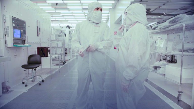
When Quazi Ummehany began her Registered Apprenticeship (RA), she was able to build that experience from the ground up at NY Creates, a world-leading R&D innovation hub and commercialization facilitator based in Albany, NY. Today, she works as a Research Support Specialist at the Albany NanoTech Complex, supporting research and development in a highly technical cleanroom environment.

As part of NAW 2026, NIICA is highlighting stories like Ummehany’s to show how apprenticeship connects people to careers while helping critical industries build the workforce they need.

We first shared her story in 2025 as she began building her career through apprenticeship. Since then, her role has grown in both scope and complexity. Read her original profile.

That progress became clear in December 2025, when she completed the Industrial Maintenance Technician (IMT) Apprenticeship Program and was promoted to the research role.

“Since the last featured story, I successfully completed the Industrial Maintenance Technician Apprenticeship Program in December 2025. The next big milestone of my journey was being recognized by NY Creates and my peers, leading to a promotion,” said Ummehany. 

Today, her work takes place inside a cleanroom environment, where precision and consistency are essential. She works across multiple toolsets, has earned certifications, and now plays a role in supporting others as they learn.
 
“I train new operators, sharing technical expertise to help them resolve complex issues and track their progress. I collaborate effectively with a diverse team of technicians and engineers,” said Ummehany.
 
Her responsibilities have shifted from following established processes to understanding how those systems function and how to improve them.
 
“As a Cleanroom Operator, the role has shifted significantly over the past year from general operator to a more tech-driven position. It has shifted from simply operating the equipment following standard protocol to a deeper understanding of the tools, technology, and the semiconductor industry as a whole,” she said.
 
That shift has changed how she approaches the work.
 
“At this stage of my journey, the most exciting part is the transition from theory to tangible production. There is immense satisfaction in starting with raw ingredients or a digital blueprint and following it through the entire process until it becomes a high-precision component,” Ummehany said.
 
Through her apprenticeship, Ummehany has developed skills across electrical and electronics systems, mechanical systems, automation and controls, and troubleshooting. She has also continued her education at Hudson Valley Community College to strengthen her capabilities in her current role.
 
Along the way, support made a difference. The Maddison Spaulding Memorial Scholarship, awarded through NIICA, helped reduce financial pressure while reinforcing her confidence.
 
“The scholarship inspired me to move forward in my career and fueled my ambition. In addition to alleviating some financial pressure, this honor and recognition have given me the confidence to pursue a life-long career in this growing industry,” she said.
 
Over time, her interests became more focused.
 
“My apprenticeship has been crucial for my career development. It helped narrow my general interest to a specific focus on semiconductor research and manufacturing industries,” said Ummehany.
 
For Ummehany, apprenticeship offers a direct and practical path into a field that can otherwise feel difficult to access.
“Apprentices learn practical, hands-on skills directly applicable to their field while earning wages. This approach helped me build professional networks and gain experience without the burden of large educational debts,” she said.
 
Looking back, the impact extends beyond technical skills.
 
“This apprenticeship program has had a transformative impact, providing me with a structured, debt-free pathway to a secure career. Most importantly, it made me more confident and self-assured in my abilities,”said Ummehany. Now, she sees her apprenticeship as the foundation for continued growth. “My apprenticeship represents the solid foundation that validated my skills and paved the way for professional advancement.”
 
Employers looking to build a stronger, more sustainable workforce with workers like Quazi, can connect with NIICA to explore how RA can support your talent pipeline strategy across critical industries.
 

Expanding Cleanroom Education Through AR/VR: Inside NORDTECH-Supported Innovative Workforce Offering

As investment in domestic semiconductor research, prototyping, and manufacturing expands, the demand for a highly skilled technical workforce has never been greater. The Semiconductor Industry Association projects 67,000 unfilled U.S. semiconductor jobs by 2030, a number that doubles when factoring in supply chain roles. To meet this challenge, the NORDTECH Hub is deploying a powerful suite of Augmented Reality (AR) and Virtual Reality (VR) cleanroom training resources that expand access, reduce barriers, and modernize how engineers, technicians, and students learn about semiconductor fabrication.

In addition, as the owner and operator of the nation’s largest and most advanced 300mm semiconductor R&D facility, NY Creates’ Albany NanoTech Complex is in a unique position to offer targeted 300mm Prototyping Fab Facility Microelectronics education. Learners are participating in workforce training at Creates, including AR/VR based training, so that they can be immersed in cutting-edge nanoscale engineering labs and cleanrooms. By interacting with 300mm wafer processing engineering and operations staff engaged in groundbreaking research, students discover diverse career opportunities in the semiconductor industry.

Read more HERE

NY Creates Showcases Global Collaboration and Innovation at SEMICON Europa 2025

NY Creates team at SEMICON Europa

The NY Creates team wrapped up a strong attendance at SEMICON Europa in Munich, Germany, and engaging with international partners, meeting new potential collaborators, and further expanding our global presence as a leader in semiconductor innovation and R&D. As the semiconductor industry becomes more interconnected than ever, this year’s conference underscored the essential role of international cooperation in shaping a resilient, sustainable future.

From the exhibit floor to technical sessions and partner meetings, Create’s leaders highlight how our organization continues to drive world-class research, strengthen global networks, and support the semiconductor ecosystem’s growth across continents.

Spotlight on Industry Sustainability Leadership

A key moment of the week was a presentation by Frank Tolic, Director of Business Development at Creates, titled “Industry Sustainability Initiatives at NY Creates.” Frank outlined how, as global semiconductor demand accelerates, the industry must pair rapid innovation with responsible environmental stewardship.

He also highlighted Creates’ Sustainability Test Bed Program, an initiative designed to help partners evaluate and scale next-generation industry sustainability solutions. From energy efficiency to water conservation and emissions reduction, the program provides a platform for collaborative research and actionable results. Frank also underscored Creates’ ongoing work with groups such as SEMI’s Semiconductor Climate Consortium, reinforcing our commitment to advancing industry sustainability.

Advancing International R&D and Workforce Partnerships

Throughout the week, the Creates team spotlighted how international collaboration continues to accelerate discovery, enhance workforce training, and build a more robust technology pipeline. Whether through cross-border R&D efforts, shared technology development, joint workforce programs, or academic partnerships, these connections are essential for strengthening the global semiconductor supply chain.

Creates presence at SEMICON Europa, showcasing how our organization is expanding its international engagement strategy and deepening relationships that directly impact innovation and sustainable growth for our partners and the broader industry.

A Growing Global Brand

This year’s conference reinforced Creates’ as a world leader in semiconductor R&D and innovation. With growing interest from organizations across Europe, our presence at this international conference reflects the increasing recognition of our cutting-edge Albany NanoTech Complex facilities. SEMICON Europa once again provided a valuable platform for bringing together industry experts, leading companies, and respected institutions committed to advancing next-generation technologies. Creates was proud to contribute to that conversation, and we look forward to building on the momentum from throughout the week into collaborative innovations that drive tomorrow’s technology.

NY Creates also plans to attend SEMICON Japan in December, participating with a booth (located in West Hall 4, W3563) and presentation.

NY Creates Showcases Innovation, Workforce Development, and Industry Leadership at SEMICON West 2025

Team NY Creates at SEMICON West 2025

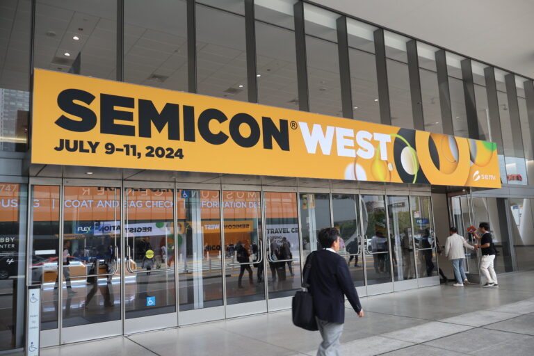
NY Creates took center stage at this year’s SEMICON West conference, participating in multiple engaging sessions that highlighted the organization’s leadership in semiconductor innovation, workforce development, and collaboration across the semiconductor ecosystem. Held in Phoenix, Arizona, SEMICON West “wrangled” together global leaders from across the industry to discuss the innovative technologies, groundbreaking R&D, and new workforce development initiatives to drive partnerships that continue shaping the future of the semiconductor industry.

Throughout the week, Creates leaders and experts shared insights on topics ranging from artificial intelligence, sustainability, workforce development and recruitment strategies, and more.

Creates President, David Anderson, moderated an executive panel titled, “Powering the Next Decade: AI’s Impact on Semiconductor Infrastructure and Market.” This robust discussion examined how artificial intelligence is transforming semiconductor design, manufacturing, and supply chain operations. Pres. Anderson was joined by a distinguished panel of industry leaders, including Angada Sachid (ASM), Mukesh Khare (IBM), Laura Matz (Merck KGaA, Darmstadt, Germany), and Mark Dougherty (Tokyo Electron US). Together, they explored how AI will drive technological advancement and reshape the semiconductor landscape over the coming decade.

Creates Vice President for Education and Workforce Development, Dr. Robert Geer, joined GlobalFoundries Workforce Development Lead, Christine McLear to present, “Building a Collaborative Regional Consortium for Semiconductor Workforce Development” at the Workforce Development session. The presentation explored how partnerships among industry, academia, and government are fueling a new generation of high-tech talent, supporting the semiconductor ecosystem, and ensuring a strong, sustainable pipeline of skilled professionals.

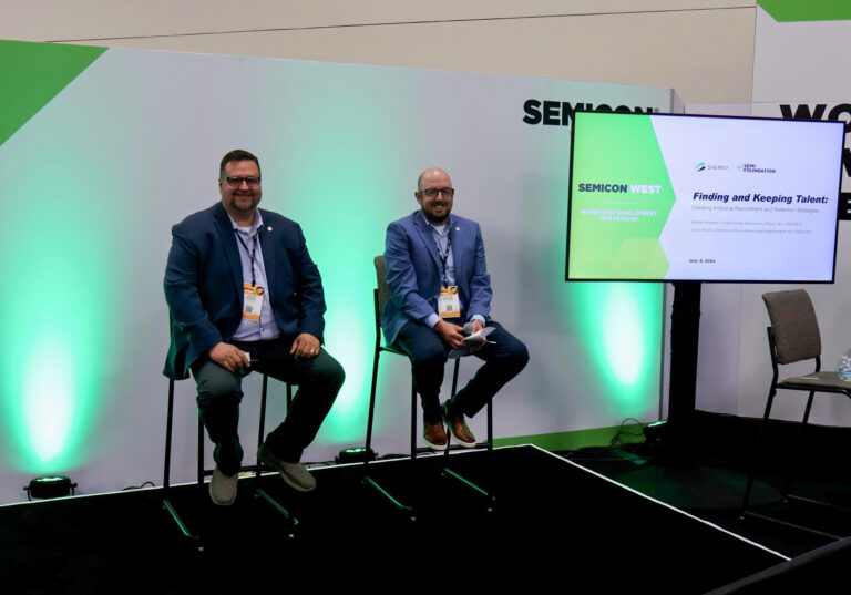
At that same session, Justin Rivers, Creates Director of Recruitment and Employment, presented “From Job Application to Onboarding: How to Lock Down the Position You Are Seeking” at the Workforce Development Pavilion. Drawing on years of experience in human resources and recruitment, Rivers shared practical advice for professionals pursuing careers in high-tech fields — including opportunities at Creates. Many in the large crowd stayed after the talk to ask Justin for his advice, with a line of interested individuals that lasted more than a half hour.

On Wednesday, Creates Sustainability Engineering Manager, Irina Spiry, took part in the SEMI Semiconductor Climate Consortium Scope 1 Working Group Gases Panel. Engaging discussions from the panel provided an opportunity for attendees to hear input on this topic and our creation of a testbed at Creates that will address important aspects of gas alternatives and abatement. 

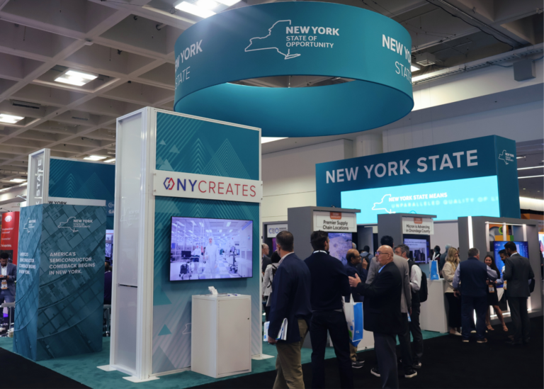
Beyond the presentations, attendees were invited to connect with Creates representatives at their booth, where the team showcased the organization’s expanding role as a hub for research, innovation, and workforce growth in semiconductors.

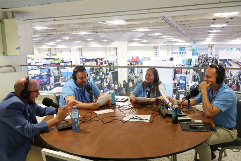
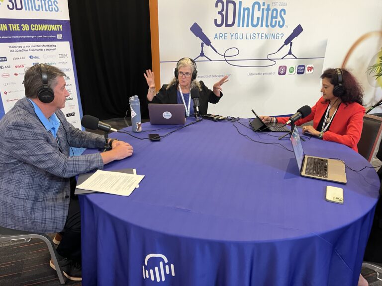
Creates also recorded live episodes of its NanoChat podcast throughout the conference, featuring exclusive interviews with industry experts on topics such as recruitment, workforce development, and sustainability. 

The Creates team extends its appreciation to everyone who stopped by the booth, attended a session, or joined a conversation. Together with its partners and collaborators, Creates continues to drive innovation, strengthen the semiconductor ecosystem, and shape what’s next for advanced technologies.

If you would like to follow up with Creates following the SEMICON West Conference, you can do so by emailing contact@ny-creates.org.

Also, stay tuned for upcoming NanoChat episodes recorded live from the SEMICON West floor, and learn more about how Creates is redefining the future of the semiconductor industry.

A Fresh Look for a Future-Focused Mission

3D rendering Albany NanoTech Complex with NY Creates logo
3D rendering of Albany NanoTech Complex with NY Creates logo

Check out Creates’ new look, with a fresh logo, updated visual identity, and new branding resources reflecting our commitment to sustainability, collaboration, and innovation.

NY Creates President Dave Anderson

“I am excited to share that we have officially launched a refresh of our organization’s logo and updated our branding guidelines, marking the  dynamic evolution of NY Creates. This rebranding reflects more than a progressive new look. It represents and highlights our continued commitment to being at the forefront of innovation and collaboration.

Our new visual design elements incorporate a vivid green, underscoring our commitment to industry sustainability while signaling a forward-looking, strategic focus on our partners, stakeholders, and the next generation of high-tech talent.”

 Dave Anderson, President, NY Creates

Accelerating Innovation

Creates’ Albany NanoTech Complex is a world-renowned hub for research and development, commercialization of nanotechnology, and semiconductor innovation. 

Located in Albany, New York, it has evolved over decades into a leading center for cutting-edge scientific exploration and a major hub for collaborating with industry partners across the globe. The 1.65 million square foot NanoTech complex boasts more than $25 billion in high-tech investments and myriad corporate partners, with approximately 3,000 semiconductor-related jobs on site.

Our core values and the foundation of Creates drives our work everyday

Integrity

Transparency, accountability, and responsible stewardship.

Collaboration

Bridging government, academia, and industry to build stronger innovation ecosystems.

Innovation

Advancing solutions that drive economic and environmental progress.

Excellence

World-class facilities and people delivering measurable impact.

Community

Nurturing future engineers and strengthening local and regional collaboration.

Check out the fresh branding on our Social Media accounts

We’re excited to introduce the new Creates visual identity, a modern logo and brand that reflects our commitment to sustainability, collaboration, and innovation across our social media channels.

Branding Contact

For questions related to the updated branding, or to request co-branded materials, please contact:

The Marketing Department | marketing@ny-creates.org

Jason Conwall, Director of Marketing and Strategic Affairs | jconwall@ny-creates.org

We’re proud to share this fresh look with our community. The brand reflects who we are, an organization powered by integrity, collaboration, and a relentless focus on innovation.

NY CREATES Welcomes MIT Microelectronics Interns for In-Depth Tour and Hands-On Experience

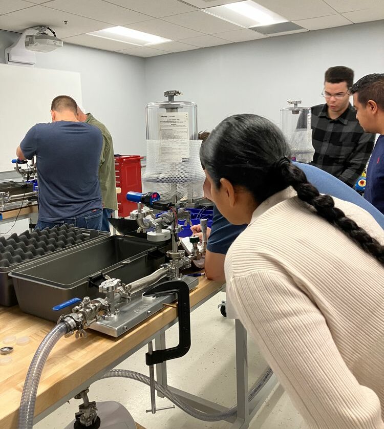
NY CREATES was proud to host students from the Massachusetts Institute of Technology (MIT) as part of the Northeast Microelectronics Internship Program, offering these future innovators a firsthand look at advanced semiconductor research and development efforts at our Albany NanoTech Complex.

With support from the Northeast Regional Defense Technology Hub (NORDTECH), the visit gave interns a comprehensive overview of the important role NY CREATES’ Albany NanoTech Complex plays in strengthening semiconductor R&D, economic advancement, and workforce development capabilities in New York and throughout the United States. During their tour, the students were joined by representatives from the Northeast Microelectronics Commons Hub (NEMC), underscoring the collaborative spirit of the Microelectronics Hubs that drives this workforce development initiative forward.

The experience included an in-depth tour of NY CREATES’ 300mm cleanroom facilities and leading-edge infrastructures, where students saw how advanced technologies are developed through public-private partnerships that span academia, government, and industry partnerships.

One of the highlights of the visit was a hands-on educational session led by an Instructional Support Technician from the University at Albany, Stephen Stewart. This educational session guided the students through the fundamentals of semiconductor processing, offering a rare and valuable opportunity to connect classroom knowledge with real-world chip fabrication techniques.

To conclude their day, the students made a final stop at GlobalFoundries in Malta, a key industry partner in the region’s microelectronics ecosystem. There, they gained additional perspective on how research transitions to high-volume manufacturing and contributes to a resilient domestic supply chain.

The MIT interns’ visit exemplifies the importance of building meaningful connections between education, research, and industry. We’re proud to support the development of the next generation of high-tech workforce, and we look forward to continuing to open doors for young minds shaping the future of trailblazing technologies.

NY CREATES Signs Five Future Cleanroom Operators at Capital Region BOCES CTE National Signing Day

Image courtesy of Capital Region BOCES

As part of the 2025 Career and Technical Education (CTE) National Signing Day celebration, NY CREATES proudly recognized five exceptional high school seniors who have committed to joining our team as Cleanroom Operators (CRO I) upon graduation.

CTE National Signing Day honors students across the country as they sign letters of intent to begin careers in skilled trades, technical fields, or continue their education—highlighting the value of hands-on learning, technical training, and direct-to-career pathways.

Each student will graduate this June from their home school district and their Capital Region BOCES CTE program, officially beginning their transition from student to skilled professional in New York’s advanced manufacturing and semiconductor workforce.

Capital Region BOCES and NY CREATES 2025 Signing Day Class:

  • Giovanni Blenman – Electrical Trades, Schenectady City School District
    Ariana Nahlupin – Cosmetology, South Colonie Central School District  
  • Tristan Szesnat – Electrical Trades, Mohonasen Central School District
    Spencer Tracy – Heating, Ventilation, Air Conditioning & Refrigeration (HVAC/R), Mohonasen Central School District
  • Hayden Hyslop – Culinary Arts and Hospitality Technology, RCS Central School District (not pictured)

These students will be offered Cleanroom Operator (CRO I) positions at NY CREATES following graduation, and we are thrilled to support their launch into meaningful careers at the Albany NanoTech Complex, celebrating their achievements in partnership with Capital Region BOCES and their home districts.

Their signing and committing to start their careers at NY CREATES reflects the power of strong education-to-career pathways and the bright future of the semiconductor industry in our region. We looking forward to welcoming these future innovators to NY CREATES soon! 

Media Coverage:

News10 ABC: BOCES students commit to jobs with area businesses

Capital Region Chamber: Capital Region BOCES National Signing Day is a Success: 40 Area Teens Sign Letters of Intent to Work in the Skilled Trades

Empowering Workforce Development and Student Innovators Through Leading-edge Tech at NY CREATES

At NY CREATES, providing opportunities for hands-on training with advanced semiconductor research tools is a significant aspect of workforce development and student education. One such tool that is now being used for research and analysis is the Bruker D8 DISCOVER Plus, an X-ray Diffractometer (XRD) used for materials characterization in both academic and industry settings.

Innovative Technology Applications

X-ray diffraction is a technique that enables the precise analysis of the structure and composition of a wide variety of materials by investigating their crystalline structure and measuring how X-rays interact with the material’s atoms.

This process allows users to identify compounds by analyzing their atomic arrangement, providing a unique “fingerprint” of the material. Thin films and layered structures can also be investigated to determine thickness, interface roughness, and density, and measurement of the internal stress of stacked layers helps ensure high-performance material properties in semiconductor applications. Analysis of a material’s crystalline quality also supports the optimization of material performance in next-generation electronics

Bridging Education and Industry 

Access to the X-ray diffractometer can be valuable for students and researchers preparing for careers in semiconductor-related fields, especially because the configuration of the instrument at the NY CREATES lab offers great experimental flexibility and fast, very reliable results. This particular instrument also has an Atlas goniometer, and a non-coplanar arm, both with very stringent specifications in terms of resolution, accuracy and repeatability, that make it one of the most advanced in the industry. 

NY CREATES provides training for students and individual researchers to operate the Bruker D8 DISCOVER Plus independently, helping them develop practical skills in materials characterization and data analysis. This experience not only strengthens their technical expertise but also enhances their career readiness, making them competitive candidates for industry roles upon graduation.

Beyond student training, this cutting-edge tool also serves as a resource for on-site partners, who are able to utilize it for high-precision data analysis of several different materials. In this way, its availability at NY CREATES’ Albany NanoTech Complex contributes to collaboration between academic institutions and industry partners.

Shaping the Future of Semiconductor Talent

As semiconductor technology continues to evolve, exposure and accessibility to innovative R&D tools remain important components of workforce development. This diffractometer is just one of several resources available at NY CREATES’ Albany NanoTech Complex that support technical training, research, and collaboration with industry and academic partners. 

Providing valuable training with these tools empowers students and researchers to develop real-world technical expertise in materials science and semiconductor engineering and serves to strengthen connections between amongst members of the site’s unique chips-focused ecosystem.