View Original News Release Here
SCHUMER, HOCHUL ANNOUNCE NEW YORK RECEIVES FIRST-EVER DEPARTMENT OF DEFENSE MICROELECTRONICS COMMONS HUB, DELIVERING $40 MILLION FEDERAL INVESTMENT – FIRST MAJOR AWARD FROM SCHUMER’S CHIPS & SCIENCE ACT – TO BOLSTER NEW YORK’S BOOMING SEMICONDUCTOR INDUSTRY AND TRAIN NEXT GENERATION OF NY’S TECH WORKFORCE TO SUPPORT AMERICA’S NATIONAL SECURITY
NORDTech, A Consortium Of NY Defense And Semiconductor Manufacturing Powerhouses Including NY CREATES, UAlbany, Cornell University, RPI, IBM And More, Is Among First In The Nation To Tap Major Fed Investment From Schumer’s CHIPS And Science Act
Schumer Created DoD’s Microelectronic Commons Program To Encourage Commercialization Of Key Tech For U.S. Microelectronics And Designers, Bringing R&D From ‘Lab To Fab’— To Launch New Companies, Support The NY Semiconductor Workforce, And Secure This Critical Technology For National Security
Schumer: We Are Building Future Of America’s Semiconductor Industry Here In NY— And Now First Major Award From CHIPS & Science Act Is Here To Supercharge New York’s Chip Companies And Workforce!
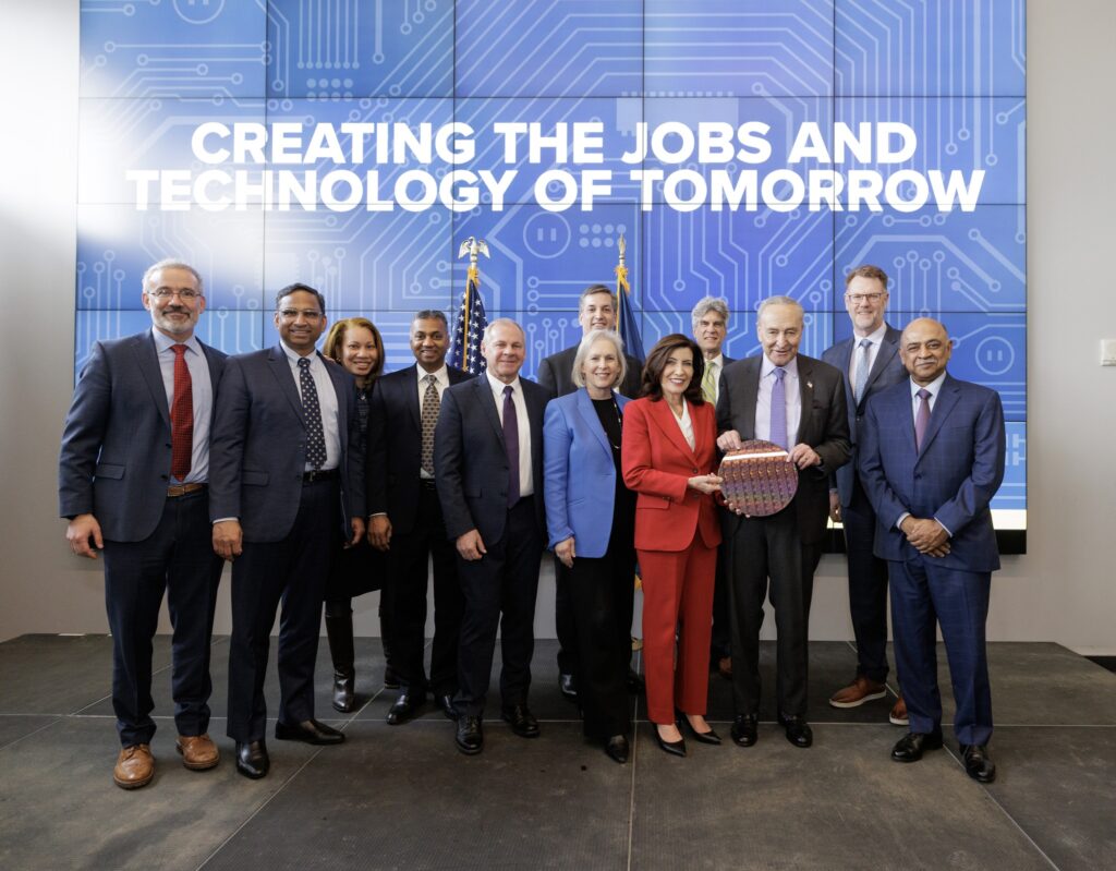
U.S. Senate Majority Leader Charles E. Schumer and Governor Kathy Hochul today announced a New York–based consortium has been awarded $40 million from the Department of Defense’s (DoD) Microelectronic Commons Program. This funding is one of the first major CHIPS awards from Schumer’s CHIPS & Science Act and will establish the infrastructure of the hub, allowing partners to bolster workforce training programs for the semiconductor industry and add new state-of-the-art microelectronics equipment.
The consortium, known as the Northeast Regional Defense Technology Hub (NORDTech), led by NY CREATES, the University at Albany’s College of Nanotechnology, Science, and Engineering (CNSE), Cornell University, Rennselaer Polytechnic Institute (RPI), and IBM, will bring together academia, industry, and government organizations to help supercharge New York’s booming chips industry to spur innovation, attract new companies, strengthen the workforce, and bolster this industry, which is vital to America’s national security.
“This first-ever Department of Defense Microelectronics Commons Hub award is booster fuel for the rocket that is Upstate New York’s booming microchip manufacturing industry. With New York as one of the first major CHIPS awards recipients, it is clear the feds are recognizing what I have long known, New York is the home of America’s semiconductor future. This $40 million Microelectronic Commons Hub will make sure research is turned into new companies and new jobs and supercharge New York’s semiconductor workforce, adding new state-of-the-art lab equipment to facilities across the state, and bringing new discoveries from lab to fab,” said Senator Schumer. “With the first major funding from my CHIPS & Science law on the way, there is no greater glowing welcome sign to say New York will be America’s semiconductor superhighway. And this is just the start! From the Capital Region to Central NY to New York City, this major award from the Department of Defense will help us seize this once-in-a-generation opportunity to invest in cutting-edge semiconductor technology and to train our workers to make major chip investments in the state like Micron and GlobalFoundries’ proposed expansion a success and ensure the next major breakthroughs for semiconductors are discovered here in New York State.”
“This transformative federal grant is not only a major investment in New York’s chips ecosystem – it’s an acknowledgment of everything we’ve accomplished so far to establish Chips Country in our state,” Governor Hochul said. “From our groundbreaking Green CHIPS legislation to Micron’s historic $100 billion commitment for a new campus creating 50,000 jobs in Central New York, we are laying the groundwork for a global hub for semiconductor businesses right here in New York State. I thank Majority Leader Schumer for his leadership in passing the federal CHIPS and Science Act and his help in securing this funding, and I look forward to a continued partnership with all of the local, state, and federal stakeholders as we advance our mission to bring the jobs and the businesses of the future to New York.”
This funding comes from the $2 billion CHIPS for America Defense Fund which Schumer helped establish in his CHIPS & Science Act. Schumer first successfully authorized the creation of the DoD Microelectronics Commons program as part of the authorization of the first-ever federal chips incentives and R&D programs in the National Defense Authorization Act (NDAA) For Fiscal Year 2021. Schumer then included in his U.S. Innovation and Competition Act (USICA) $52 billion in mandatory funding to implement these incentive and R&D programs, including $2 billion for the DoD Microelectronics Commons program. After passing the Senate in June 2021, USICA was eventually combined with similar House-passed legislation to become the CHIPS and Science Act, which was signed into law in August 2022.
Schumer wrote to Defense Secretary Austin in support of the consortium and pulled out all the stops to deliver this support for NORDTech, including also personally calling the Defense Secretary to advocate for the proposal. He explained that with the funding, NORDTech, along with over 60 regional partners across the Northeast, will leverage their resources to sustain technology leadership and strengthen the New York regional ecosystem in semiconductors. NORDTech was one of eight hubs selected nationwide.
The $40 million in Department of Defense funds announced today will establish the NORDTech Hub infrastructure and processes. This will include new semiconductor-focused capital equipment located at several NORDTech member sites across New York State, as well as the people and processes that will rapidly make these key capabilities easily accessible to NORDTech members who conduct DoD-prioritized technical projects and workforce training opportunities. The membership includes NY CREATES at the Albany NanoTech Complex, University at Albany, Rennselaer Polytechnic Institute, IBM, Cornell University, the Griffiss Institute, Mohawk Valley Community College, the NY CREATES Test Assembly and Packaging (TAP) facility located in Rochester, Brookhaven National Laboratory, and many more.
As an awardee of this competition to help establish the national Microelectronics Commons, the NORDTech Hub enables its member participants to pursue further funding through subsequent DoD funding opportunities for multi-million-dollar investment in microelectronics prototyping projects and workforce development activities. The senator said this investment is a force multiplier in New York State, because those small, medium, and large employers can then use the distributed NORDTech Hub in the Microelectronics Commons network to achieve technical project goals and workforce goals, helping launch next-generation semiconductor-based technology in a range of industries, and is delivering a once-in-a-generation opportunity to launch rewarding, highly skilled careers across the semiconductor supply network in New York State.
Schumer said this funding will also help lay the groundwork to ensure ongoing semiconductor projects are a success and to land additional federal funding for opportunities like becoming the major hub of the National Semiconductor Technology Center (NSTC) in the Capital Region at NY CREATES’ Albany NanoTech Complex. Schumer has long said that the Albany NanoTech Complex is the most “shovel-ready” R&D facility in the country and ready to quickly stand up the NSTC. The multibillion-dollar Albany NanoTech Complex is the most advanced, publicly-owned, 300-millimeter semiconductor R&D facility in North America, has well-established partnerships with industry leaders, workforce training providers, and top academic research institutions across the country, including in critical logic and packaging capabilities, and is set up to immediately begin supporting the needs of the broader semiconductor ecosystem, including startups, small businesses, and the workforce. The site and its partners have a long record of accomplishment of groundbreaking research that has led to successful technology transfer, translating research into manufacturing.
Schumer has fought tirelessly to uplift the Capital Region and Upstate New York as a major hub to lead the nation in semiconductor manufacturing and research. Early this year, Schumer personally invited NY CREATES President David Anderson to President Biden’s 2023 State of the Union address to highlight his push to land the NSTC in the Capital Region. Prior to the passage of the CHIPS and Science Act, Schumer not only brought the Commerce Secretary to Malta to highlight opportunities for expansion at GlobalFoundries and across Upstate New York’s semiconductor industry, but also arranged for Secretary Raimondo to meet with NY CREATES and industry leaders, including from IBM and Applied Materials, to discuss the unique assets the region has for leading the NSTC. Schumer also brought Commerce Deputy Secretary Don Graves to Albany to tour the Albany NanoTech Complex and see firsthand how the Capital Region is perfectly suited to stand up the NSTC and begin boosting the nation’s semiconductor industry.
The DoD’s Microelectronic Commons, funded by Schumer’s CHIPS and Science Act, is a network of microelectronics R&D infrastructure investments, including facilities, support for an ecosystem of companies of all sizes, and workforce development designed to empower industry and researchers in working with the DoD’s efforts in microelectronics development. With the creation of regional ecosystems funded by the DoD program, each focusing on key technology areas, the Microelectronics Commons will close the gap between research ideas and realization of those ideas, translating more research into new technology, new companies, and expansion of existing companies. The Commons is designed to enable sustained partnerships between emerging technology sources, manufacturing facilities, and interagency partners. It also works to develop a pipeline of talent to bolster local semiconductor economies and contribute more broadly to the growth of a domestic semiconductor workforce. Learn more at www.nordtechub.org.
Empire State Development President, CEO and Commissioner Hope Knight said, “Under Governor Hochul’s leadership, New York State is building for the future with strategic investments in next-generation technologies and workforce development to promote sustainable economic growth. This Department of Defense grant – and the collaborative efforts of the NORDTech partners – will strengthen our continued buildout of this dynamic industry, and we’re grateful to Senator Schumer and our federal partners for their support.”
Dave Anderson, President of NY CREATES said, “On behalf of NY CREATES, we are extremely grateful for the incredible leadership of Senate Majority Leader Schumer and Governor Hochul, who have both laid the groundwork for this exciting announcement through their continued delivery of strategic semiconductor-centered investments which have contributed to U.S. competitiveness while making our state the preeminent innovation hub in the nation. As a result of today’s announcement, we look forward to building the Northeast Defense Technology Hub in the Microelectronics Commons region in and around New York State with our partners, including the University at Albany’s CNSE, Cornell University, Rensselaer Polytechnic Institute, and IBM. Initiatives like this are not only significant in and of themselves, but they also further foster growth of New York’s established high-tech ecosystem by leveraging our world-class semiconductor-focused resources, capabilities, and facilities to secure the future of microelectronics for the nation.”
“New York is home to one of America’s premier semiconductor ecosystems, delivering breakthroughs that have made chips more powerful, smaller, greener and ready for the era of artificial intelligence. IBM is proud to play a key part in that ecosystem alongside several of New York’s world class research universities. Our work together in this new Department of Defense Microelectronics Commons Hub will solidify the state’s role at the forefront of chip innovation. This leadership only happens through the hard work of leaders like Majority Leader Schumer, Governor Hochul and others,” said Arvind Krishna, Chairman and CEO of IBM.
“This is tremendous news for Upstate New York and for the next generation of high-tech talent across the state,” said Heather Hage, President, and CEO of Griffiss Institute. “Today’s announcement would not have been possible without the tireless legislative work of Senator Schumer on last year’s CHIPS and Science legislation, and we thank him for his continued advocacy to help grow New York’s high-tech economy. I would also like to thank Governor Hochul for her support of our vision for NORDTech, as well as the vote of confidence shown in our region by the Pentagon. This new investment by our nation’s military demonstrates clearly that Upstate New York has what it takes to build the workforce of the future in highly secure, leading-edge semiconductor technology. I’m proud the Griffiss Institute will contribute to this effort by leveraging our work with the Air Force Research Laboratory Information Directorate to help connect the Department of Defense with the world-class research and education capabilities across New York, with a focus on leading high-tech small businesses in emerging technologies such as quantum information science that will be critical to the next generation of microelectronics.”
“NORDTech is a great example of how academia, companies of all sizes, and economic development teamwork will enhance the future of the semiconductor industry in the U.S.,” notes Krystyn J. Van Vliet, Vice President for Research & Innovation at Cornell University. “Cornell appreciates the strong support of Senator Schumer and Governor Hochul to grow this field of research, discovery, translation and inclusive workforce creation across New York, and recognizes the contributions of the many researchers, technical staff, and organizations who built the NORDTech proposal to the Department of Defense. We look forward to working together to convert the potential energy of the MicroElectronic Commons Hubs into the kinetic energy of prototyping and outcomes for new semiconductor-intensive technologies and the expanded workforce that will create them.”
SUNY Chancellor John B. King, Jr. said, “Our thanks to Senate Majority Leader Schumer and Governor Hochul for providing the leadership and direction needed to drive growth in semiconductor research and development across our state. SUNY’s colleges and universities, powered by NY CREATES and UAlbany’s CNSE, are well positioned for this opportunity because we have state-of-the-art facilities hosting groundbreaking research, excellent faculty and researchers creating innovation, and strong workforce development programs preparing New Yorkers for in-demand careers. We are grateful for the significant investment announced today, and proud of our role in the NORDTech consortium.”
University at Albany President Havidán Rodríguez said, “This is extraordinary news for the Capital Region, and the University at Albany is proud to be a part of the consortium that will strengthen and expand New York’s semiconductor sector. Albany NanoTech was early proof of the wisdom of NORDTech’s ‘lab to fab’ approach to microelectronic and semiconductor materials research, and CNSE has been an integral part of that success for nearly two decades. Now, thanks to the leadership of Sen. Schumer, Gov. Hochul and NY CREATES, UAlbany-CNSE stands ready to help ensure New York and the nation remain at the leading edge of semiconductor advances.”
Martin A. Schmidt, Ph.D., President of Rensselaer Polytechnic Institute said, “The next generation of microelectronics will be born in New York State. We are proud to be among the founding members of this consortium and are ready to get to work with our partners in higher education, industry, the Capital Region and beyond to make New York a leader in chips innovation. We thank Senator Schumer and Governor Hochul for their continued support and leadership to make this vision a reality.”
“I knew the CHIPS and Science Act would be a game-changer for our region — already a hub of innovation — to become the center of semiconductor resurgence for our nation and a key driver in this critical industry,” Congressman Paul Tonko said. “That’s why I pushed hard to advance this key legislation alongside Majority Leader Schumer and our leading semiconductor manufacturing institutes. I’m thrilled to see this critical investment now being delivered. This funding, made possible through our CHIPS Act, will enable our centers of research, learning, and development to explode in potential, strengthening our economy and creating good paying jobs right here in our region and beyond. As we celebrate this historic announcement, I will continue pushing for federal action to deliver on the promise of a high-tech innovation economy hub in the Capital Region.”
“As a member of the House Appropriations Committee, I’ve fought for federal investment opportunities in innovation for our community,” said Congressman Joe Morelle. “This investment out of the CHIPS & Science Act is an exciting step forward in the fight to reestablish the US as a global leader of innovation, and it is no surprise the Finger Lakes Region is included in the first major award. I’m grateful to Senator Schumer for his leadership and collaboration and look forward to continued regional investments.”
###