
For Immediate Release: Monday, June 17, 2024
Contact:
Steve Ference |sference2@ny-creates.org | +1 (518) 424-6029
Eun Kyong Choi | ekchoi@nnfc.re.kr | +82 (42) 366-2061
Albany, N.Y. and Daejeon, Korea – NY CREATES, a non-profit focused on semiconductor-based R&D, workforce development, and economic advancement, and the National Nano Fab Center, the leading public organization for providing semiconductor technology services in Korea, announced a partnership which aims to develop a shared hub for enabling joint research, aligned technology services, testbed support, and an engineer exchange program to bolster chips-centered R&D, workforce development, and each nation’s respective high-tech ecosystem.
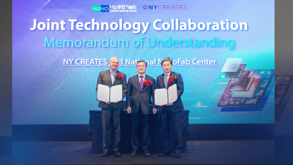
Leaders from the New York Center for Research, Economic Advancement, Technology, Engineering, and Science (NY CREATES), based in Albany, New York, and the National Nano Fab Center, which is based in Daejeon, South Korea, met at a series of engagements in Korea in early May when NY CREATES President Dave Anderson and NNFC President Park Heung Soo ceremonially signed the agreement. The two organizations plan to work together to grow the U.S.—SouthKorea semiconductor research ecosystem, including the expansion of prototype production and demonstration. As part of the visit, NY CREATES leaders also took part in the 20th anniversary celebration of NNFC’s operations.
This partnership news follows U.S. Senate Majority Leader Charles Schumer’s announcement that he secured a commitment from South Korea President Yoon Suk Yeol for Korea to partner with NY CREATES for advanced semiconductor R&D at its Albany NanoTech Complex. This also builds upon a joint declaration signed in 2023 to promote collaboration and partnership between NY CREATES and the Korea Institute for Advancement of Technology (KIAT). Such partnerships highlight NY CREATES’ fast-growing collaborative network, amplifying its role as a premier global center for semiconductor research and as an ideal major hub for the National Semiconductor Technology Center (NSTC) which is to be established under the U.S. CHIPS & Science Act.
“This exciting new partnership between NY CREATES and Korea’s National Nano Fab Center will further strengthen New York’s booming semiconductor hub. When I met with President Yoon last year, he personally agreed to growing Korea’s partnerships with New York, including in the microchip industry, and now we are going to hit the ground running towards a shared vision of the future powered by an innovation economy we are building together,” said Senator Schumer. “International partnerships like this show why Albany NanoTech is best positioned to be a major hub of the National Semiconductor Technology Center created by my CHIPS & Science Law. By creating a shared hub for semiconductor research, workforce development, and more, this partnership marks another step forward on Upstate NY’s collaborative efforts to build out the region as a global chips leader.”
“NY CREATES is proud to congratulate the National Nano Fab Center as they celebrate 20 years of operations. Now, we look forward to developing a collaborative hub for technology development services and testbed support that will leverage the capabilities of our globally recognized Albany NanoTech Complex, America’s most advanced 300mm semiconductor research center, and the resources of the NNFC’s state-of-the-art facilities,” said NY CREATES President Dave Anderson. “This global partnership will identify synergistic areas of research and promote advancements in the semiconductor field that are critical for our allied nations to ensure continued technological strength.”
“We are very pleased to announce the collaboration of NNFC and NY CREATES as joint semiconductor technology hubs for the industry and semiconductor researchers in Korea and the U.S. We will actively support bilateral semiconductor research and open up new opportunities for the industry,” said NNFC President Park Heung Soo.
At a conference held May 9 in Seoul, NY CREATES met with key members of the Korean semiconductor industry and their partners. There, more than 200 participants heard NY CREATES leadership team present an overview about the organization’s world-class capabilities and its related business opportunities. In addition, nearly three dozen companies participated in separate face-to-face business discussions with the NY CREATES business team, leading to active discussions with multiple Korean semiconductor companies large and small about potential collaboration.
Following the Seoul visit, NY CREATES’ leadership team visited Korea Advanced Institute of Science and Technology (KAIST) in Daejeon, Korea, to tour the campus and participate in NNFC’s 20thanniversary celebration. A number of Korean dignitaries attended, including Vice Minister of Science and ICT Lee Chang Yoon and KAIST President Lee Kwang-Hyung.
Paul Kelly, NY CREATES Vice President of Strategies, Partnerships, & New Ventures and Chief Operating Officer presented to the more than 300 participants, sharing that while NY CREATES’ name indicates the organization is based in New York State, “we are focused on enabling meaningful global partnerships.”
This latest international partnership announcement also follows New York Governor Kathy Hochul’s December announcement: a $10 billion partnership composed of IBM, Micron, Applied Materials, Tokyo Electron, and others to establish a next-generation semiconductor research and development center at NY CREATES’ Albany NanoTech Complex. Once built, New York’s High NA EUV Lithography Center will position the state as a destination for research and development of innovative chip technology and foster international partnerships as world-renowned research organizations expand their presence in the U.S.
###############
About NY CREATES
NY CREATES serves as a lab-to-fab bridge for advanced electronics, fostering public-private and industry-academic partnerships for technology development and innovation. NY CREATES attracts and leads industry-connected innovation and commercialization projects that secure significant investment, advance R&D in emerging technologies, and generate the jobs of tomorrow. NY CREATES runs some of the most advanced facilities in the world, boasts more than 2,700 industry experts and faculty, and manages public and private investments of more than $20 billion—placing it at the global epicenter of high-tech innovation and commercialization. Learn more at www.ny-creates.org.
About National Nano Fab Center
NNFC started as a KAIST-affiliated institution, located on the KAIST campus in Daejeon, South Korea. NNFC was established in May 2004 and this year marks its 20th anniversary. Since 2014, NNFC has been affiliated to Ministry of Science and ICT in Korea, providing technology services with advanced facilities in the field of semiconductor, nano-bio, MEMS and display, etc. NNFC also fosters semiconductor top talents, especially for college graduates. As NNFC stared its service in 2005, the total number of R&D services by NNFC is more than 220,000 and about 8,900 institutions including academia and industry have used the NNFC technical services and facilities. NNFC provides top-notch technical services with 200mm and 300mm semiconductor equipment as well as various MEMS tools, growing into a global leading public institution for supporting R&D activities and commercialization at home and abroad. Learn more at www.nnfc.re.kr/eng/
###
News Coverage:
Times Union: NY CREATES to partner with South Korean version of Albany NanoTech


