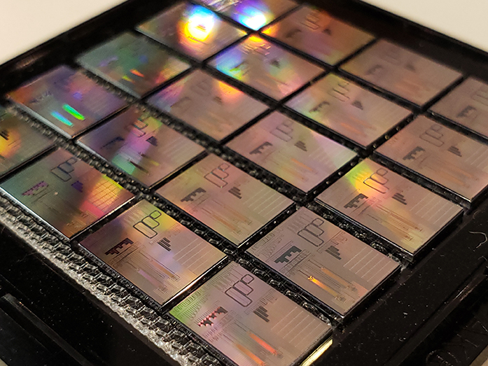
This project will establish a first-of-its-kind capability at 300mm wafer scale that will lead towards scalable quantum computing devices, with higher performance characteristics.
AIM Photonics celebrates its 5th anniversary
AIM Photonics enters fifth year with over 120 members, industry leading MPW program, PDK, and first ever world-class open-access 300mm wafer test, assembly and packaging facility online and accepting customers. In celebration of AIM Photonics 5 year anniversary and the technical achievements, AIM Photonics and DoD partners present a look into the institute. The national broadcast on Information Matrix will be hosted by award-winning actor Laurence Fishburne on more than 200 public television stations beginning the week of May 25, 2020, and features some of the incredible innovations and applications of integrated photonics.
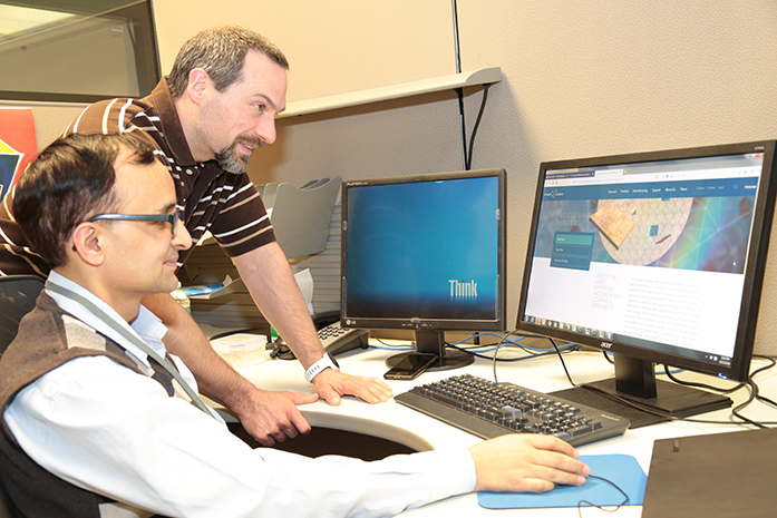
AIM Photonics announces latest version of PDK v3.5 addressing Design for Manufacturability
AIM Photonics PDK v3.0 announced. Industry leaders recognize AIM PDK as industry leading. The release of Process Design Kit (PDK) v3.5 Compact Model Library sponsored by AIM Photonics is the first to support statistical models in Lumerical’s INTERCONNECT, introducing a set of statistical models based on the measured wafer-scale data of photonic components.
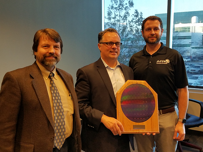
AIM Photonics produces first fully integrated 300mm Quantum Photonic wafer
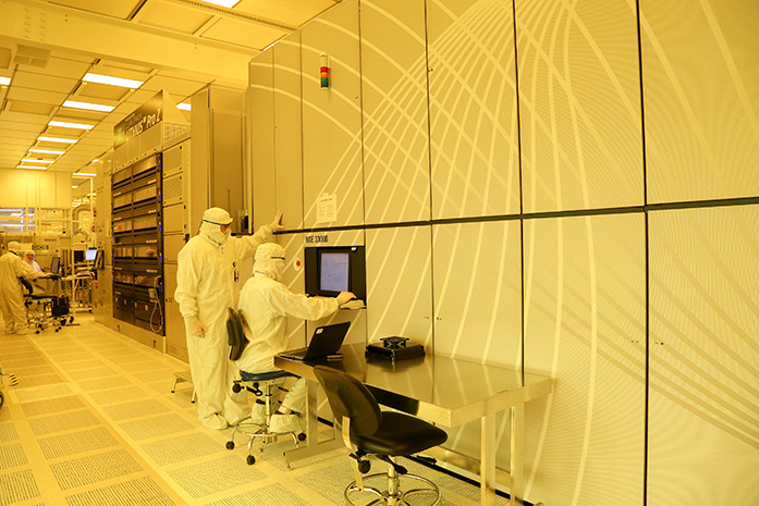
The quantum photonics wafer project is led by the Air Force Research Laboratory and RIT. The wafer includes chip designs from both RIT and Air Force Research Laboratory, along with designs by collaborators at MIT, Purdue University, Oak Ridge National Laboratory, Army Research Laboratory, and Rensselaer Polytechnic Institute. The wafer was fabricated by AIM Photonics in NY CREATES’ advanced 300mm microelectronics facility in Albany, N.Y.
Letter of Intent signed to join the Quantum Economic Development Consortium (QED-C)
QED-C is one of the premier initiatives of the National Quantum Initiative, an industry-driven consortium run by SRI, and supported by the National Institute of Standards and Technology
Governor Andrew M. Cuomo announces that IBM plans to invest over $2 billion to grow its high-tech footprint at the Albany campus and throughout New York State.
Governor Andrew Cuomo announces a $2 billion investment by NYS and IBM to grow the company’s high-tech footprint at NY CREATES and throughout New York State. New York State invests $300 million over five years to support the the establishment of an “AI Hardware Center” for artificial intelligence-focused computer chip research, development, prototyping, testing and simulation.
Over 2000 students complete first online PIC design course
Air Force Research Laboratory awards grant to develop devices for neuromorphic computing
AIM Photonics Announces Best-in-Class 300mm Silicon Photonics Multi-Project Wafer (MPW) Performance
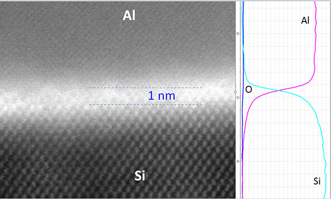
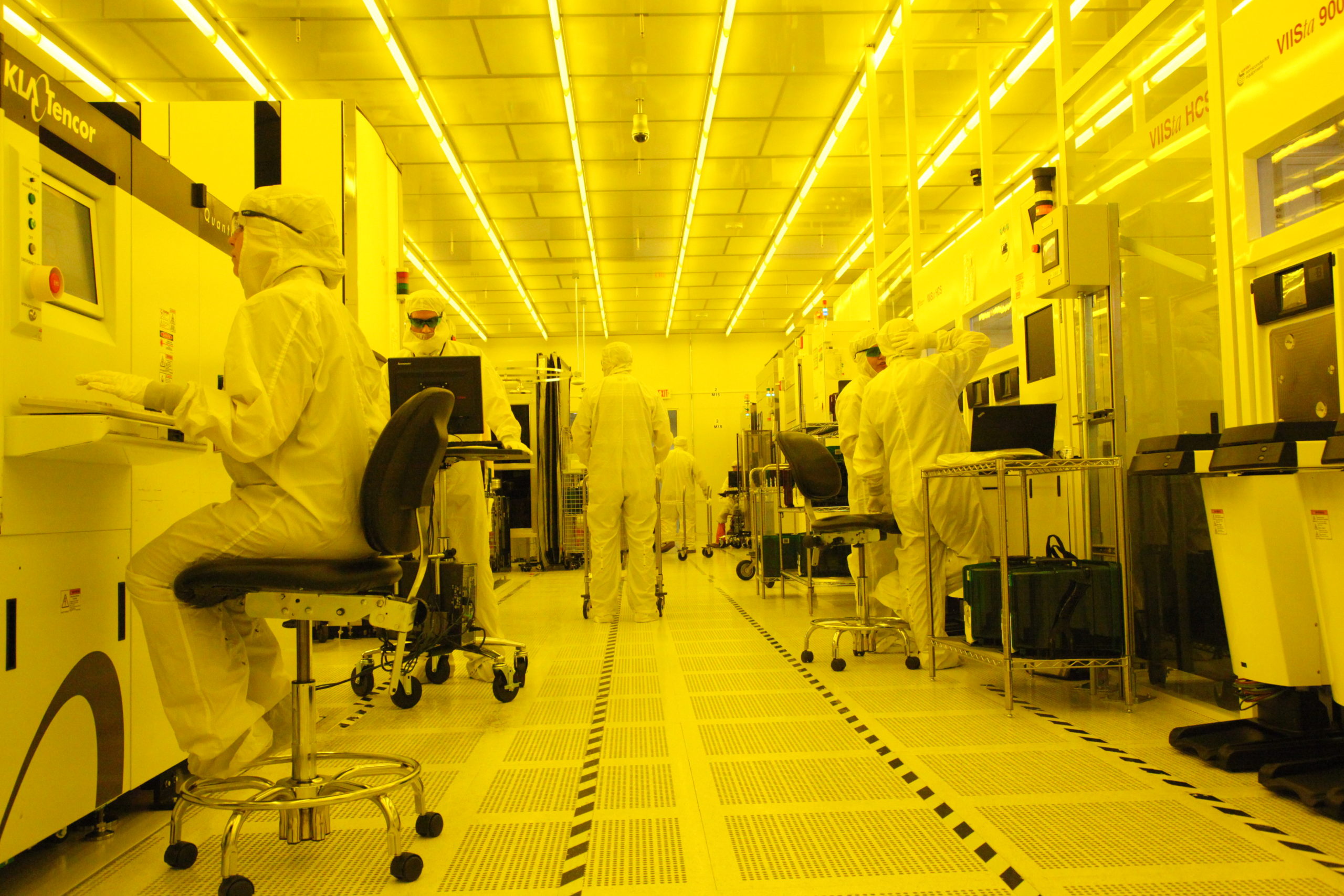
AIM Photonics superior MPW performance is the result of new, ultra low-loss waveguides, featuring attenuation that is less than .25 and .10dB/cm for 220nm silicon and 220nm silicon nitride (SiN), respectively, in addition to around 1dB/facet edge coupler for both transverse electric (TE) and transverse magnetic (TM) polarization. With only 90-day fabrication time for full actives to be processed on 300mm silicon on insulator (SOI) wafers, and using the same toolset that produces 14nm and smaller circuits, these capabilities also enable easy transfer to similar high-volume equipped foundries if needed.
NSF Awards $1.2M to AIM Photonics and academic partners to advance key technology programs
Academic institutions partner with AIM Photonics to realize advanced computing architecture using light; develop mobile probes for identifying specific materials; and enable improved manufacturing processes for photonic devices. Rochester Institute of Technology, University of California-San Diego, University of Delaware to Leverage AIM Photonics’ World-Class R&D and Foundry Capabilities.

