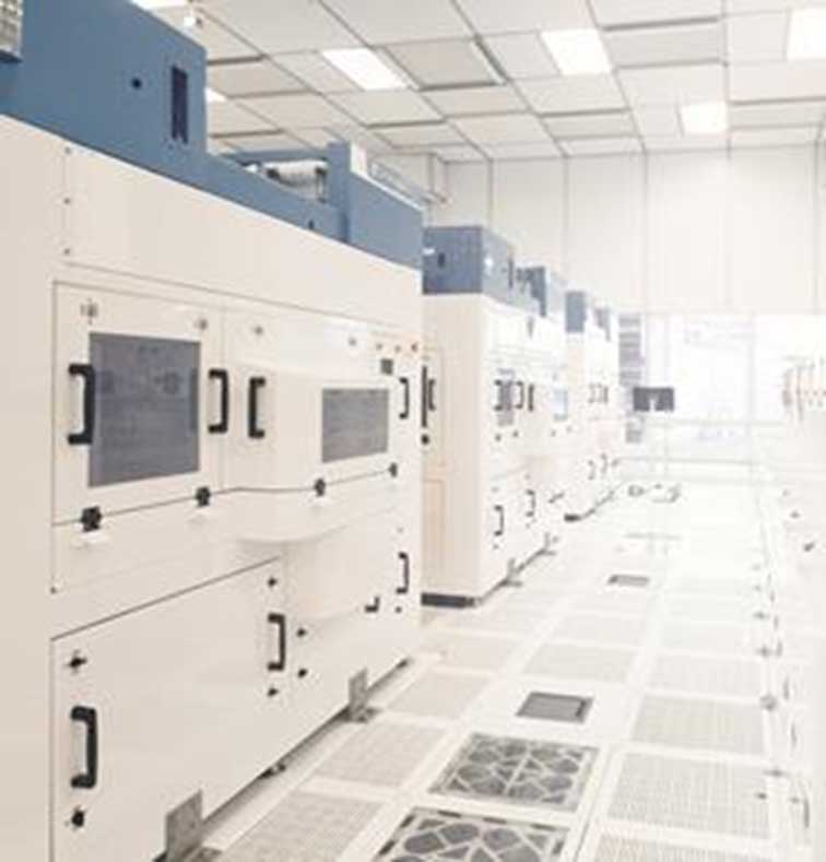
The META Center is a $850 million new R&D institute at NY CREATES in Albany. New York State will invest $250 million to leverage a $600 million, seven-year commitment from Applied Materials to fund materials engineering R&D, prototyping and pilot projects in fields like virtual intelligence, augmented and virtual reality, semiconductors and advanced optics. (Image courtesy Applied Materials)
AIM Photonics announces program to develop a CMOS-compatible waveguide platform for integrating MWIR and LWIR laser sources
The $1.7 million U.S. Department of Defense (DoD) project will support a consortium of AIM Photonics members led by University of California Santa Barbara (UCSB) and includes Northrop Grumman, the U.S. Naval Research Laboratory, and SUNY Polytechnic Institute. The majority of development to date has focused on a relatively narrow wavelength range —around 1550nm. The goal of this government-directed project is to address the opportunities at longer wavelengths.
AIM Photonics Members develop Sarin Gas Sensor
AIM Photonics announces latest version of PDK to address High-Speed Optical Communications (50Gbps)
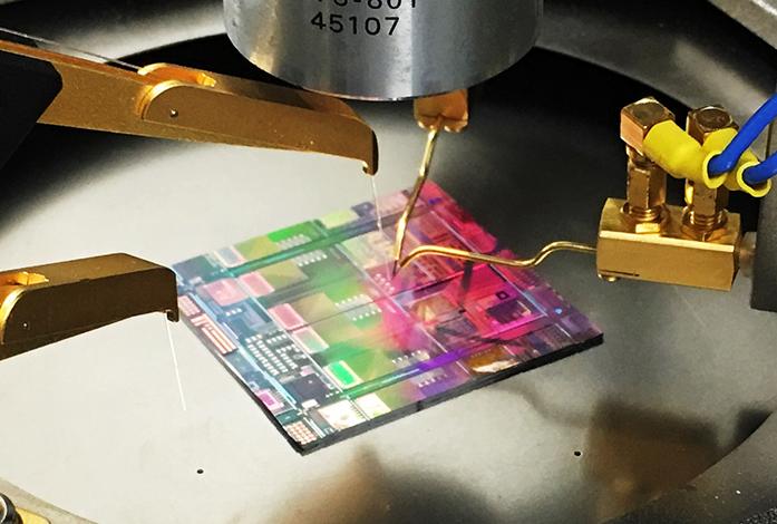
In this release, Analog Photonics (AP) expanded the comprehensive set of Silicon Photonics Integrated Circuit (PIC) component libraries within SUNY Poly’s process to address the high-speed optical communication needs. Combined with Multi-Project Wafer (MPW) runs, this PDK will give AIM Photonics members access to world-class silicon photonics components.
Commonwealth of Massachusetts invests in AIM Photonics and burgeoning integrated photonics industry across the Northeast
January 11th, 2018 Worcester Polytechnic Institute and Quinsigamond Community College announced they would receive $4 million for a second LEAP facility on WPI’s campus. The LEAPS are funded by the Commonwealth of Massachusetts Manufacturing Innovation Initiative (M2I2) program to support AIM Photonics.
First Photonic Integrated Chip (PIC) technology transfer program begins
AIM announces participants of DoD sponsored integrated photonic cryogenic datalink for focal plane arrays
Integrated Photonics workforce development programs begin
Construction of AIM Photonics Test, Assembly and Packaging (TAP) facility begins
AIM Photonics launches its premiere Lab for Education & Application Prototypes (LEAP)
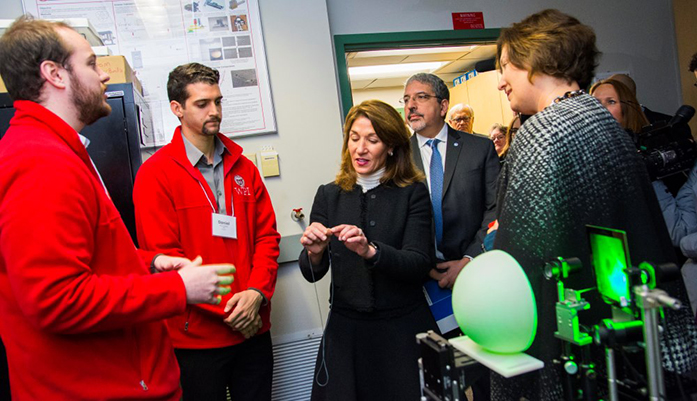
AIM Academy launched its Lab for Education & Application Prototypes (LEAP) on MIT’s campus in the spring of 2017. The LEAPS are funded by the Commonwealth of Massachusetts’ M2I2 program to support AIM Photonics. They will enable (1) the fabrication of prototypes and initial proof of manufacturing and (2) the creation of new high-tech integrated photonics manufacturing jobs.

