NY CREATES Announces New AIM Leadership

NY CREATES (New York Center for Research, Economic Advancement, Technology, Engineering and Science) announce the appointment of Dr. Michael J. Cumbo as Chief Executive Officer (CEO) for the American Institute for Manufacturing Integrated Photonics (AIM Photonics), a program of NY CREATES, effective July 6, 2020.  Dr. Cumbo succeeds Dr. Michael Liehr in the role.

AIM Photonics is the nation’s premier Photonic Integrated Chip (PIC) manufacturing institute advancing Integrated Photonic technology and workforce innovation. A public-private partnership, founded in 2015, AIM Photonics is celebrating 5 years of success and is nationally recognized for creating the world’s first open-access complete Integrated Photonic manufacturing ecosystem, which provides the photonic community and DoD access to a full suite of advanced technology, capabilities, and resources throughout the entire product development cycle.

“The AIM Photonics executive team is pleased to welcome Dr. Cumbo, a highly experienced and accomplished technology executive, as the next leader of this important manufacturing institute,” said Dr. Douglas Grose, President of NY CREATES.  “Mike brings valuable experience to AIM Photonics as a results oriented, customer-centric technology business leader, in addition to his proven ability to move technology and teams ‘from lab to fab,’ and transforming new technologies into profitable businesses.”

Empire State Development Acting Commissioner, and President & CEO-designate Eric Gertler said, “AIM Photonics is advancing New York State’s leadership in optics, photonics and imaging by attracting industry innovators from across the globe, building on Governor Cuomo’s targeted Upstate investment that has grown the Finger Lakes region as an OPI industry hub. Dr. Michael Cumbo’s experience and leadership will no doubt help AIM to further expand its presence both statewide and around the world and we are pleased to officially welcome him aboard as the consortium’s new CEO.”

“As we celebrate AIM Photonics’ 5 year anniversary, and look to the next 5 years, what better way to celebrate than to welcome back to Rochester, Michael Cumbo,” said Mr. Ed White, National Photonics Initiative Chairman and Associate Vice President for AIM Photonics Test, Assembly, and Packaging (TAP) facility in Rochester, NY.  “AIM Photonics will benefit significantly from Mike’s technology leadership expertise, and I look forward to working with him to continue the advancement of the TAP facility and sharing his vision for the next 5 years and beyond.”

Prior to his new role, Dr. Cumbo was Vice President of Optics for ZYGO Corporation, a unit of AMETEK, which designs, develops and produces complex electro-optical systems and high-precision optical components for the Medical/Life Sciences, Defense & Aerospace, Semiconductor, and Industrial OEM markets.  He had full P&L responsibility and drove significant improvements in the business during his tenure.  He is the Founder and Chairman of Sandia Electro-Optics Corporation (SE-OC), Albuquerque, NM, an employee-owned enterprise devoted to the incubation of innovative measurement instruments in the life science and environmental sensing market segments. 

Previously, Dr. Cumbo spent 30+ years managing various levels of photonic technology development across the globe, most recently as President of IDEX Optics & Photonics.  He also spent time as a key advisor and expert supporting improvement programs for a number of venture capital startups.  Prior to that, Dr. Cumbo managed various photonics based companies including; Executive Vice President and General Manager, Coherent, Inc., Vice President and General Manager, Uniphase Commercial Laser Division, Vice President of R&D and Chief Technical Officer, OCLI, Vice President and General Manager, OCLI Telecom Division, as well as a number of management and engineering positions with OCLI, Bausch & Lomb, and Eastman Kodak in his home town of Rochester, NY. 

Dr. Cumbo holds a Ph.D. in Optics, an M.S. in Optical Engineering, and a B.S. in Physics from the University of Rochester (UofR), as well as an M.S. in Electrical Engineering from Rochester Institute of Technology (RIT).  He has 11 patents, and authored 22 technical journal papers and conference proceeding articles.  He was chosen to announce the Prism award by SPIE at Photonics West 2012. 

NY CREATES COO Mr. Paul Kelly said, “AIM Photonics is leading how integrated photonics are developed and built and we’re proud to have such an exceptionally qualified leader to continue the program as part of the NY CREATES family, especially during AIM’s fifth anniversary.  We look forward to Mike leading the charge and taking AIM Photonics and Integrated Photonics to the next level.”

“I am excited to be joining the talented team at AIM Photonics, the nation’s premier Integrated Photonic manufacturing institute,” said Dr. Cumbo. “The recent innovations and applications demonstrated by AIM Photonics are already changing the world as we know it.  I’m honored to continue the efforts and look forward to expanding the technological opportunities in my home town of Rochester, NY, as well as within the state of New York and across the nation.”  

A vital component of NY CREATES is AIM Photonics, with more than 120 members, including those focused on data communications, sensors, quantum and neuromorphic computing.  AIM featured services include our industry leading Process Design Kit (PDK), Multi Project Wafer (MPW), and Test, Assembly and Packaging (TAP), which include a comprehensive set of silicon Photonic Integrated Circuit (PIC) devices enabling the implementation of next-generation products.

Dr. John Bowers, Deputy CEO of AIM Photonics, and distinguished professor of Electrical and Computer Engineering and Materials at University of California Santa Barbara (UCSB) said, “We are just beginning to see the significant impact AIM Photonics is having on the world of integrated photonics.  There is so much more to accomplish, and it is a pleasure to have an individual of Mike’s qualifications leading us through the next phase.”

Dr. Cumbo will open the AIM Photonics 2020 Summer Members Meeting which is scheduled for July 15th, at 2:00PM (EST).   Details on the upcoming Members Meeting and additional events can be found at the AIM Photonics events website. http://www.aimphotonics.com/new-events

SEMICONDUCTOR DIGEST 2020/06/22

At 5-Year Mark, AIM Photonics Looks Back on Key Accomplishments, Future Goals

ROCHESTER, N.Y., June 16, 2020 — Since 2015, AIM Photonics has been at the forefront of New York’s success in the integrated photonics arena. Over the past five years, AIM has created a photonic integrated chip (PIC) manufacturing ecosystem, providing the photonics community with access to advanced technology, capabilities, and resources throughout the entire PIC product development cycle, from design, proof of concept, piloting, and development, to final test, assembly, and packaging, prior to commercialization.

This ecosystem has enabled small- and medium-size businesses, which would otherwise be priced out of the market, to bring integrated photonic chip (IPC) technologies through the product development cycle. Members  (there are over 120) and partners can use the resources provided by AIM without incurring prohibitive costs or risking more than they can afford. AIM’s test assembly and packaging (TAP) facility in Rochester, N.Y. — one of the organization’s primary achievements during its first five years — is the only 300-mm photonic packaging research facility in the world with open access.

“The test assembly and packaging facility is key to advancing the technology,” Ed White, AIM Photonics associate vice president and National Photonics chair, said. “Allowing companies to have access to the means to get their photonics product to market is something that doesn’t exist anywhere else in the world, except in privately owned facilities.” The cost of developing a chip is very high, and assembly and packaging easily make up one-half of that cost, White said.

Ed White (left), associate vice president of AIM Photonics TAP facility and National Photonics Initiative chairman, describing how a 300-mm wafer is tested in the analytical lab. 


The TAP facility makes it possible for small companies that may need only one chip on a wafer to develop and produce only what they need. “We help them get in the game by giving them access to very expensive technology,” White said. “Their minimum run can be what they need it to be — one chip or 10 or 50. We can provide the means to package for as many or as few wafers as needed.” TAP has development and production process capabilities in wafer scale, chip scale, and I/O attach. The facility has state-of-the-art test and metrology capabilities for each of these functional areas.

AIM’s IPC development team in Albany, N.Y., is available to help AIM Photonics members with their IPC designs. The photonics member community can access design libraries created by AIM and then transfer that design to the chip development team in Albany. After the PIC is made, it’s transferred to the TAP facility for final test, assembly, and packaging.

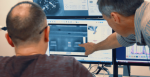
AIM Photonics TAP engineer testing wafer in the analytical lab.
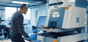
 

The AIM ecosystem — composed of the Process Design Kit (PDK), Multi Project Wafer (MPW), private and custom wafer runs, and the TAP facility — has led to significant advancements in PIC technologies over the past five years. “Many industry, government, and academic partners have stated that without the ecosystem, some of the current advancements would not have been possible for another five to 10 years,” Frank Tolic, chief marketing officer, said. Developments facilitated by the AIM ecosystem during its first five years include quantum photonic chips; advances in biomedical and biochemical sensors; optical transceivers that today perform at the speed of 400 to 800 Gb, and that in the future will perform at Tb speed; radio frequency (RF) over fiber applications; and lidar on a photonics chip.

Photonics in the Time of COVID
By drawing on its experience in managing product timelines and scaling production, AIM Photonics was able to respond quickly to the pandemic, submitting a proposal to the U.S. Department of Defense (DoD) to be one of the first to support research in testing for the SARS-CoV-2 virus. AIM is helping industry, the DoD, and research labs collaborate on sensors for the testing, with the goal of having new sensors on inexpensive silicon chips by 2020-2021 flu season. While initial commercial rollout will be to clinical laboratories, the ultimate goal is to have a point-of-care SARS-CoV-2 test for use wherever flu tests are offered. AIM is facilitating a collaboration between the University of Rochester and Ortho Clinical Diagnostics to develop sensors for SARS-CoV-2 testing, and is partnering with researchers at SUNY Polytechnic Institute on the development of microfluidic devices for use in testing for SARS-CoV-2. 


Helping Lockheed Realize RF over Fiber Solutions for Its Platforms
Lockheed Martin is working with AIM Photonics to improve RF over a fiber network. Integrated photonics will allow the company to use more compact chips, reducing size and weight and saving power. IPCs will give its data communications more bandwidth and scalability. The business will be able to respond to new requirements quickly, without the need to re-cable, by moving existing fiber cabling to a different frequency and using multiplexing to put multiple sources of information on a single fiber. Lockheed has been a member of AIM Photonics since 2017.


Engineers analyzing AIM Photonics device structures in chips at TAP analytical lab.


AIM is working to extend its funding agreement with the DoD and the contracting process it uses in support of the congressional plus-up program. New York State has made a strategic investment in AIM Photonics, providing $250 million in funding. “A large portion of that was spent on the TAP facility in Rochester, on new metrology tools and equipment that is now being used by our members,” Tolic said.

In the next five years and beyond, AIM will seek to advance the IP ecosystem it has created through continued collaboration with its members and partners. Some existing and new technologies that AIM will focus on could include new PDKs for specific technologies such as sensors, packaging, and quantum. AIM will continue to welcome and support new ideas and collaborations from industry, academia, and government. It also intends to expand educational programs for PIC technology and applications, with a focus on expanding these programs to community colleges and undergraduate programs across the U.S.

Recently installed new equipment at Rochester, N.Y., TAP facility.


The AIM Photonics TAP facility continues to engage with existing and future clients. The TAP facility is currently engaged with more than 20 customer projects and is in discussions with a number of other organizations about future work. The interest in the AIM Photonics TAP facility is high among the photonics community. “Nearly half of the people who visited us at the last nonvirtual conference, Photonics West 2020, had a primary interest in the AIM Photonics TAP facility,” Tolic said. “We are working with several Rochester-based companies and universities, including Ortho Clinical, Syntec, L3Harris, Mosaic, UR, and RIT, and new companies are looking to work with us, especially in the areas of sensors and datacomm.”

If you are interested in learning more about how the AIM Photonics ecosystem can help you bring your idea for a photonics product to market, visit http://www.aimphotonics.com/info-request. Your information will go directly to the AIM Photonics business development team. 

ROBIN RILEY, WEB EDITOR
ROBIN.RILEY@PHOTONICS.COM

https://www.photonics.com/Articles/At_5-Year_Mark_AIM_Photonics_Looks_Back_on_Key/a65863

Photonics.com
Jun 2020

NY CREATES Celebrates Fifth Anniversary of AIM Photonics

Albany, NY, June 04, 2020 (GLOBE NEWSWIRE) — The New York Center for Research, Economic Advancement, Technology, Engineering and Science (NY CREATES) today announced AIM Photonics will be featured on the nationally broadcast educational program Information Matrix as part of its fifth anniversary celebration.  Formally established as the American Institute of Manufacturing Photonics in 2015, AIM Photonics has been at the forefront of New York’s success in the Integrated Photonics arena.

More than a decade ago, Department of Defense and DARPA funds were first committed to photonics programs at the Albany Nanotech site.  Industry collaboration and creative partnerships have driven this technology focus forward, as the next realm of integrated photonics design and devices are being developed at AIM Photonics facilities at NY CREATES in Albany and Rochester, NY, including the AIM Test, Assembly, and Packaging (TAP) facility.

The national broadcast on Information Matrix will be hosted by award-winning actor Laurence Fishburne on more than 200 public television stations beginning the week of May 25.  This segment was filmed on location at the TAP facility in Rochester, NY, the only open 300mm state-of-the-art photonic packaging research center in the world.  The video features some of the incredible innovations and applications of integrated photonics.

National Photonics Institute Chair Edward White said, “AIM Photonics represents the best in American innovation, leveraging the talent and expertise of some of New York’s best colleges and universities to develop new disruptive technology.  I’m excited to celebrate AIM’s fifth anniversary with this dynamic television program and hope to have even more exciting achievements to celebrate when AIM turns ten!”

NY CREATES COO Paul Kelly said, “AIM Photonics is leading a national charge to rethink how photonics are developed and built and we’re proud to have the program as part of the NY CREATES family.  This video program highlights the incredible innovations taking place at AIM Photonics and NY CREATES.  We’re proud to celebrate AIM’s fifth anniversary and look forward to the rest of the nation learning about the unmatched opportunity for collaborative partnerships and advancement here in New York.”

With public and private investment of more than $400 million, AIM Photonics has achieved a number of milestones in its five years, including:

  • Engaging with industry partners to advance telecom/datacom, Photonic Integrated Circuit (PIC) sensors, RF Analog applications, PIC based LIDAR, and advanced photonics packaging research in 2016;
  • Establishing the first qualified integrated photonic Process Design Kit with major EPDA partners in 2017;
  • Launching a national photonics multi-project wafer to advance commercialization opportunities in 2018;
  • Securing membership from more than 120 companies and organizations;
  • Producing the first-ever quantum photonic wafer for the Air Force Research Lab and the Department of Defense in 2019
  • Beginning operations of the first-ever open 300mm photonic packaging research facility 2018
  • Developing new integrated photonic sensors to advance COVID-19 tests on a global scale 2020

As a conduit for Empire State Development and the State University of New York, NY CREATES builds on the success of the State’s ongoing investment in programs such as Albany Nanotech, AIM Photonics, and SUNY Polytechnic Institute.  More recently, NY CREATES has worked to secure major research and industry investments in New York from Applied Materials, IBM, and Cree Wolfspeed.

A vital component of NY CREATES is AIM Photonics, with more than 120 members, including those focused on data communications, sensors, quantum and neuromorphic computing.  AIM featured services include industry leading Process Design Kit (PDK), Multi Project Wafer (MPW), and Test, Assembly and Packaging (TAP), which include a comprehensive set of silicon photonic integrated circuit (PIC) devices enabling the implementation of next-generation PIC technologies.

AIM Photonics Chief Marketing Officer Frank Tolic said, “Today, as New York continues its leadership role in photonics, power electronics, and semiconductors, it is vital to share that story with the nation.  As AIM celebrates our fifth anniversary, we are thrilled to tell the world about how this industry and investment is changing the world in which we live.”

Attachments

Frank Tolic
NY CREATES
518-795-0111
FTolic@sunypoly.edu


How the Empire State is bridging the divide between academia and industry to enable job growth and innovation

Thursday, June 25, 2020
10:00 AM Pacific / 1:00 PM Eastern

For More Information

Overview:

For more than three decades, New York State has aggressively invested in the advanced electronics and thin film industries, driving new partnerships, innovation, products, and economic opportunity.  This strategic investment has included the bipartisan support of 4 governors, building the global R&D focus of what is now known as NY CREATES – more than $15 billion invested, 200+ research partner organizations, more than 150,000 square feet of clean room, and leveraging more than 2700 experts from industry, government and academia.

AGENDA:

1:00-1:05pm       Introduction: Pete Singer, Editor-in-Chief, Semiconductor Digest
1:05-1:10pm       Opening Remarks and Welcome: Doug Grose, President NY CREATES
1:00-1:20pm       NY State of Opportunity: Empire State Development
1:20-1:30pm       NY CREATES Overview: LaMar Hill, NY CREATES
1:30-1:45pm       Future Quantum Technology Trends and Company Case Study:
                           S. Papa Rao, NY CREATES and Oleg Mukhanov, co-CEO SeeQC
1:45-1:55pm       AIM Photonics-TAP: Ed White NY, CREATES
1:55-2:00pm       Wrap-up: Paul Kelly, COO NY CREATES
2:00-2:15 pm      Round Table Discussion