CSIS Report: Albany NanoTech’s Potential to Support the National Semiconductor Technology Center

Aerial image of the Albany NanoTech Complex
The Albany NanoTech Complex
Report by Charles Wessner & Thomas Howell
Published, Feb. 14, 2025

The CHIPS and Science Act of 2022 (CHIPS Act) was critically important for halting and reversing the erosion of U.S. semiconductor manufacturing capability and ensuring the security of the domestic chip supply chain. Through a combination of federal grants (up to $39 billion) and tax incentives (in excess of $46 billion), the CHIPS Act has stimulated billions of dollars in private sector investments into U.S.-based semiconductor manufacturing.

The CHIPS Act established the National Semiconductor Technology Center (NSTC), an industry-government-academic collaboration meant to drive advanced semiconductor research, development, and workforce training.

In July 2024, the Department of Commerce and the recently created National Center for the Advancement of Semiconductor Technology (Natcast), the nonprofit operator of the NSTC, began the site-selection processes to identify the first three NSTC flagship facilities:

    • An administrative and chip design center.

    • An extreme ultraviolet light (EUV) lithography center will provide participants with the ability to utilize the most advanced lithography tools to facilitate the development of chips at the leading-edge of semiconductor technology, specifically those needed to support artificial intelligence applications.

    • A prototyping and advanced packaging piloting facility will combine state-of-the-art 300-millimeter (mm) manufacturing with chip prototyping and packaging, set to be operational in 2028.

The Commerce Department and Natcast conducted separate site selection processes for each facility. Selection criteria included the presence of a thriving semiconductor ecosystem at the proposed sites, with secondary considerations including chip industry presence; the availability of skilled workers; the number and quality of relevant worker training programs; the number and quality of nearby university research programs focusing on microelectronics; the amount of public and private chip investments in the preceding decade; and the number and type of benefits, incentives, and initiatives aimed at the semiconductor industry.

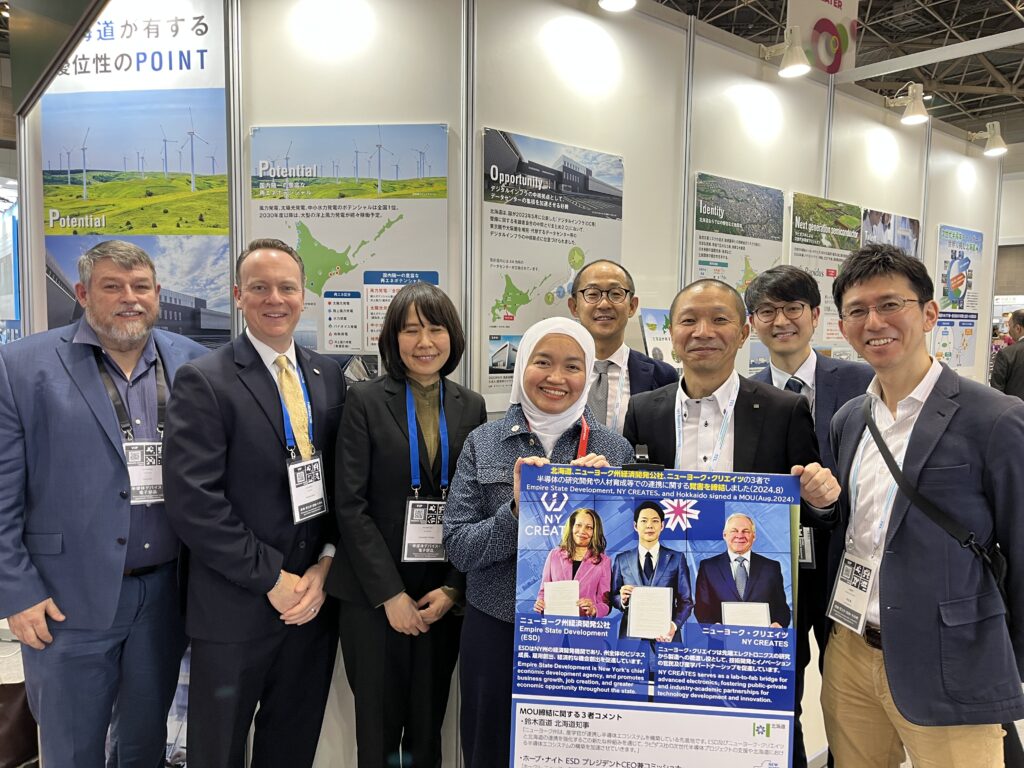
In July 2024, in a bid by the state to secure the designation of the facility as one or more of the NSTC’s foundational centers, $1 billion was invested into the semiconductor research facility at the New York Center for Research, Economic Advancement, Technology, Engineering, and Science’s (NY CREATES) Albany NanoTech Complex—hereafter referred to as Albany NanoTech.

Indeed, reflecting its unique advantages, in October 2024, the Department of Commerce and Natcast designated Albany NanoTech as the first NSTC research and development facility. Specifically, it will serve as the NSTC’s EUV lithography center, supported by a proposed federal investment of an estimated $825 million. The center is expected to begin initial operations in 2025.

In the following months, the Department of Commerce and Natcast also announced that the Design and Collaboration Facility would be established in California, while the Prototyping and National Advanced Packaging Manufacturing Program (NAPMP) Advanced Packaging Piloting Facility would be established at Arizona State University.

The selection of Albany NanoTech as the site for the NSTC’s EUV lithography R&D center validates New York’s investments in Albany. It was not lost on observers that Albany NanoTech was the first of the three NSTC flagship facility sites designated by the U.S. government, with Silicon Valley coming in second, signaling “a major shift in the center of power in the U.S. computer chip industry.” David Anderson, the president of NY CREATES, observed that the federal action was “a recognition and solidification of the Albany NanoTech center and NY CREATES as a national resource. We really are a gem for this industry and the capabilities that we have here.”

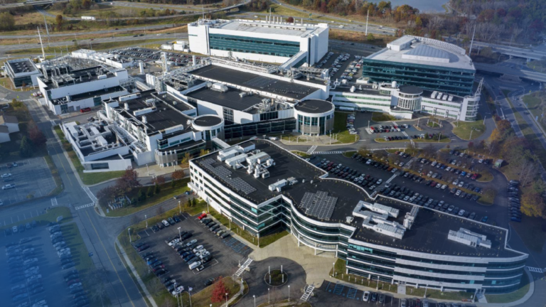
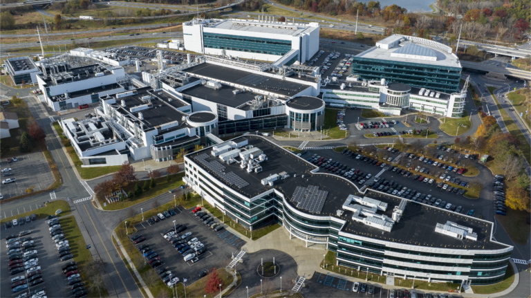
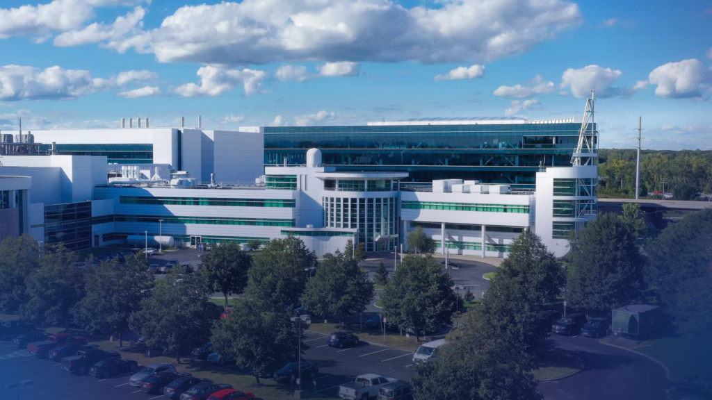
NY CREATES Albany NanoTech Complex

While the perspectives offered by Anderson might be brushed off as the sort of local boosterism commonly associated with site selections for major federal projects, his case for Albany NanoTech is grounded in a number of fundamental realities. While not fully appreciated, especially in Washington, Albany NanoTech stands at the epicenter of a long-standing, thriving semiconductor research and manufacturing ecosystem with few parallels in the United States, or worldwide. Albany NanoTech brings together cutting-edge facilities, actively engaged partners from leading device manufactures and equipment suppliers, collaborative research relationships with leading universities, and a state government already making the significant capital investments needed for such a facility to remain state-of-the-art. Key features of this remarkable institution include the following:

    • Exceptional Facilities and Tools: Albany NanoTech offers the best—if not the only—publicly available, neutral site capable of fully supporting the proposed NSTC EUV lithography center. Indeed, besides Belgium’s imec, Albany NanoTech is the only global research center scheduled to receive the newest ASML High-NA EUV machine, set to be installed in a new facility currently under construction. Albany NanoTech is the only such recipient in North America that is not a major private firm.

    • Bipartisan State Government Support: The New York state government’s support for the promotion of local semiconductor research and manufacturing has been unwavering for decades, involves billions of dollars in public outlays, and remains rock-solid. It is a leading priority of Governor Kathy Hochul.

    • Large-Scale Private Investments: The public and private sector have undertaken massive investments in chip manufacturing and research in the Albany area for the past decade. Most recently, GlobalFoundries announced an $11.6 billion expansion of its Fab 8 in Malta, New York, beginning in 2025. Additionally, the recently announced investments at Albany NanoTech include another $10 billion in public and private investments.

    • Existing High-Quality Workforce: Over 10,000 people in the Albany area are already directly employed in semiconductor research, manufacturing, supply chain, and specialty construction companies and institutions.

    • Exceptional Educational InfrastructureRead More 

NY CREATES featured in CBS6 News Story: “NY CREATES strengthens global microchip industry with diverse international collaborations”

Paul Kelly, NY CREATES Chief Operating Officer on learning and collaborating with other countries on building the nanotechnology and semiconductor industry.  

“So we want to provide this expertise and knowledge on how to fabricate them, how to build some circuits out of them on top of what we can do here to have them fabricated here,” he said.

These partnerships extend to the Netherlands, Japan, Korea, Taiwan, and more; they’re part of the bigger picture, strengthening the world’s microchip industry.

“So it brings a whole diverse aspect to the engineering background and the technology focus,” said Paul Kelly, NY CREATES COO. “So between the people they have there and our good engineers here, we’re able to work together to create this technology that will advance things that will be in your devices from your cars to your phones to every piece of technology going forward.”

Arcadis News Release: Arcadis to Design and Build Expansion for NY CREATES’ Albany NanoTech Complex

Aerial image of the Albany NanoTech Complex

The project underscores Arcadis’s expertise in semiconductor and advanced technology facility design

ALBANY, NY – January 27, 2025 – Arcadis, a global leader in intelligence-driven sustainable design, engineering, and consultancy solutions, is pleased to announce the formation of the DPS | Gilbane Joint Venture, comprised of Arcadis’s DPS Advanced Technology Group Inc. and Gilbane Building Company as the design builder and contractor for the expansion project at the Albany NanoTech Complex, which is owned and operated by non-profit NY CREATES.

This project is centered on construction of the NanoFab Reflection building (NFR), the newest addition to the New York Center for Research, Economic Advancement, Technology, Engineering, and Science’s (NY CREATES’) infrastructure. NFR will be a state-of-the-art, four-story research and development facility housing a new 50,000 SF ISO 5 cleanroom with accompanying sub-fab. The Albany NanoTech Complex expansion extends beyond the ultramodern NFR building itself to a new 900-car parking garage, and a high voltage switchyard upgrade. The Joint Venture awarded the design of the facility to Arcadis and its consultants including Dedicated Process Architecture and Engineering Services, D.P.C.

Once complete, NY CREATES, with key industry, government, and academic partners, will operate this new $10 billion High NA EUV Lithography Center to enable development of the world’s most advanced computer chips and drive the long-term growth of New York’s high-tech economy while creating and retaining thousands of direct and indirect jobs.

NY CREATES is dedicated to fostering innovative chips-focused R&D, the expansion of technology jobs in New York State, and related workforce development through industry-connected innovation and commercialization projects, such as the NanoFab Reflection project initiative. Semiconductors play a crucial role in driving the global economy, and with the impressive growth of its Albany NanoTech Complex, NY CREATES is actively contributing to encouraging innovation in an essential technological domain, paving the way for next-generation computer chips that are faster and more energy efficient.

Dr. Christopher Borst, Vice President of Technology & Infrastructure at NY CREATES, said: “Arcadis, under the DPS|Gilbane joint venture, has been entrusted as a strategic partner to design and build NY CREATES’s new NanoFab Reflection building and parking garage as well as expand critical infrastructure at our Albany NanoTech Complex. An on-time project delivery will propel next-generation semiconductor advancements for years to come.”

Michael Schwarz, Business Director, U.S. Semiconductor at Arcadis, said: “Current and future OEM tenants will benefit from this campus expansion, driving further development of new generation semiconductor tools and processes. NY CREATES’s Albany NanoTech Complex continues to be a global hub of advanced semiconductor research, and our team is excited to continue our partnership on this campus.”

Arcadis, DPS Advanced Technology Group, and Dedicated Process Architecture and Engineering Services will provide comprehensive services to the Joint Venture including architecture, engineering, procurement, logistics, and construction management personnel for the project. By establishing an interactive environment that integrates the client with the design team process, early decision-making and dynamic dialogue will positively impact all phases of the project.

The Joint Venture team will utilize modular and off-site manufacturing to achieve design to target value. They will help promote improved safety and quality and significantly reduce cost and schedule to delivery. Employing advanced planning and scheduling, the construction management team will create integrated teams to help eliminate waste and produce a highly reliable and visible schedule.

Nilesh Parmar, U.S. Places Business Area Leader at Arcadis, said: “The NanoFab Reflection project provides an opportunity to showcase multiple facets of Arcadis’s capabilities in this space including construction management and design. The impact of this expansion will be noticeable throughout the R&D technologies and the burgeoning semiconductor industry, creating future site development opportunities.”

NY CREATES’ Women’s Innovative Network (WIN): Celebrating A Year of Collaboration and Community

Cultivating a Collaborative Company Culture 

NY CREATES’ Women’s Innovative Network (WIN) enjoyed a meaningful year of partnership and community-building in support of company initiatives, promoting sustainability and charitable causes in 2024. Founded in July 2023, WIN’s members continue to cultivate a positive company culture through a focus on inclusion and collaboration at its educational events, which empowers the staff at NY CREATES and strengthens bonds that extend beyond the workplace. 

2024 Events: Positive Partnerships and Community Suppor

WIN kicked off 2024 with its International Women’s Day Networking Event, bringing together NY CREATES staff from across the organization, as well as guests from our partners at the Albany NanoTech Complex, to honor workplace achievements and milestones. The event’s international theme, Inspire Inclusion, focused thoughtful conversations about breaking barriers, sharing experiences and encouraging networking to connect the next generation of innovators. This celebration set the tone for a year dedicated to creating opportunities for staff and fostering collaboration

In the Spring, WIN turned its focus to sustainability and inspiration with an Earth Day Awareness Recycling Event and a Movie Viewing Party. NY CREATES staff united to recycle old electronics and dispose of excess electronic waste. The event demonstrated our organization’s commitment to sustainability stewardship, reducing our carbon footprint, and creating a positive environmental impact. WIN also hosted a special movie viewing party featuring the documentary, Mercury 13. This inspiring film drove stimulating conversations and deep discussions about company culture and inclusion following the film.

In the Summer, WIN also hosted its annual Speed Networking Lunch, which provided a unique opportunity to connect with fellow professionals, share ideas, and expand our NY CREATES employee network in a dynamic and supportive setting.

Throughout the fall, WIN hosted a Watch Party for SEMI’s Women in Semiconductor (WiS) Conference. This engagement gathered global leaders in the semiconductor industry to provide insightful discussions and impactful presentations about advancing diversity and collaboration in high-tech companies. As the year wound down, WIN brought holiday cheer with its Holiday Gift Donation Drive and a Holiday Cookie Swap. These events not only supported families in need but also offered opportunities for employees to come together in the spirit of giving.

Looking to 2025

As we reflect on a year of celebration and milestone achievements, WIN’s engaging employee events aim to continue to show how collaboration and connection can build bridges, inspire belonging, empower teams, and enhance the organization’s positive company culture.

CEG Press Release: NY’s 1st Nanotech Engineering Technician Apprenticeship Trade Gets Approval


Jan. 17, 2025 – The New York Department of Labor (NYS DOL) recently approved the Nanotechnology Engineering Technician (NET) trade, the first of its kind in the state, sponsored by the Center for Economic Growth (CEG).

CEG’s leadership in developing the trade creates new and expanded Registered Apprenticeship Programs (RAPs) for the region, and the state. It also helps grow the semiconductor workforce in the Capital Region and beyond, directly benefiting GlobalFoundries’ (GF) chip fab in Saratoga County and the New York Center for Research, Economic Advancement, Technology, Engineering, and Science (NY CREATES) in Albany County, both of which are initial program signatories. 

NET apprentices will get on-the-job training at GF’s manufacturing facility in Malta, in addition to related classroom instruction at Hudson Valley Community College’s Troy and Malta campuses. As the group sponsor, CEG will be responsible for the administration of NYS DOL-required apprenticeship onboarding, reporting as well as overseeing apprentices’ progression through the program. NYS DOL approved the NET RAP on Dec. 17.

“Nanotechnology Engineering Technician rounds out the suite of semiconductor industry trades that the Center for Economic Growth has been developing for the last four years. From operators and technicians in manufacturing settings to working in R&D labs, the highly skilled apprentices we are sponsoring will help further solidify the Capital Region’s status as a global semiconductor hub with the trained talent needed to continue to grow. We are grateful for the support of our partners, especially the National Institute for Industry and Career Advancement (NICCA), The Manufacturers Association (MACNY), HVCC, and New York State Department of Labor,” said CEG Chief Economic Development Officer Katie Newcombe.

“GlobalFoundries’ industry-leading registered apprenticeship program has helped GF bring new technicians into the industry and is essential for building a unique skillset that is critical to semiconductor manufacturing,” said Kerry Wright, GlobalFoundries’ Vice President of Talent Acquisition. “The addition of the Nanotechnology Engineering Technician trade creates additional opportunities for technician training at GF, further developing the technician career path, and providing additional opportunities for existing employees. We are grateful for CEG’s partnership on registered apprenticeship and leadership in developing this new trade.”

“We’re proud to be a part of this initiative, and we see this program as an integral component of our workforce development strategy,” said NY CREATES Vice President for Education and Workforce Development, Dr. Robert Geer. “Working with our partners, we intend to create pathways for individuals throughout the region to pursue careers in the semiconductor industry, as we enable leading-edge chip R&D and commercialization, economic advancement, and workforce development for New York State and the nation.”

The addition of the NET trade continues CEG’s pioneering sponsorship of career pathways for the semiconductor industry and leadership in helping companies establish and grow RAPs. In 2020, CEG became the sponsor of a first-of-its-kind RAP for the semiconductor industry to train for GF, in partnership with HVCC and MACNY. In 2023, CEG also sponsored the nation’s first semiconductor-specific RAP for a major semiconductor R&D center, in partnership with NY CREATES, the non-profit owner and operator of the Albany NanoTech Complex, and NIICA. 

Since launching its apprenticeship program in 2018, CEG has sponsored 18 signatories (employers), 122 apprentices, and supported 17 trade titles. CEG is part of the statewide Manufacturing Intermediary Apprenticeship Program partnership, which is led by MACNY. The NYS DOL Registered Apprenticeship Program is a formal training program that combines on-the-job training with formal classroom education to prepare individuals to enter and grow in new careers. CEG also acts as a Group Program Sponsor for NIICA’s Growing Apprenticeships in Nanotechnology and Semiconductor (GAINS) RAP, which will help provide incentives for company’s apprenticeship programs, including NY CREATES and GF. 

“I applaud the Center of Economic Growth (CEG) for sponsoring this revolutionary apprenticeship program, officially expanding the New York registered apprenticeship model into Nanotechnology. The CEG has been a long-time partner of the Department through their Advanced Manufacturing programs, and this new apprenticeship will help to train our workforce in the high-tech fields that will continue to shape our economy in the future,” said New York State Department of Labor Commissioner Roberta Reardon.

“MACNY is proud to partner with CEG and the members of the Manufacturers Alliance of New York to expand Registered Apprenticeship across New York State. Thanks to these efforts, the Nanotechnology Engineering Technician trade will allow for new opportunities to upskill our workforce in the jobs for tomorrow, especially as New York firmly establishes itself as a national leader in semiconductor and nanotechnology manufacturing,” said MACNY Executive Vice President Michael Frame.

“The approval of the Nanotechnology Engineering Technician apprenticeship in New York reflects the state’s leadership in building a world-class workforce for the semiconductor and advanced manufacturing industries. New York is setting a powerful example by aligning training opportunities with industry needs, paving the way for meaningful careers and long-term economic growth,” said Mike Russo, President & CEO of NIICA. “At the National Institute for Industry and Career Advancement™, we’re honored to partner with CEG and others through our Growing Apprenticeships in Nanotechnology and Semiconductors™ (GAINS) program, to support the development of NET occupation and apprentices in gaining the skills and experience they need to thrive. This initiative isn’t just about filling jobs—it’s about creating a stronger, more resilient future for individuals, businesses, and communities.”

“Hudson Valley Community College is committed to the future of workforce training in the Capital Region, and we’ve been expanding our programming, partnerships and facilities to offer more opportunities for students to prepare for the well-paid, in-demand jobs that local employers need filled, especially in areas like skilled trades and applied technologies,” said Hudson Valley Community College Officer in Charge Louis Coplin. “The creation of the Nanotechnology Engineering Technician trade and the programming that will go with it is a perfect example of how collaborating with business and community partners and organizations can benefit all of us and help create a brighter future for our region.”

About CEG

The Center for Economic Growth (CEG) is dedicated to driving economic growth in New York’s eight-county, 1.1-million-person Capital Region. As a nonprofit regional economic development organization, we do this by attracting investment and talent; growing manufacturing and workforce capabilities, leveraging industry clusters, and developing the entrepreneurial ecosystem. We serve as a catalyst and work with partners and stakeholders to prepare the region to compete and move high-impact strategies and projects forward. An affiliate of the Capital Region Chamber, CEG is supported by investors in business, government, education, and the nonprofit sectors who are committed to sustainable economic growth and shared prosperity. For more information on CEG, visit www.ceg.org.

###

DPS|Gilbane, A Joint Venture: Strategic Partnership Created to Deliver Landmark Expansion Project at Albany NanoTech Complex for NY CREATES

The Albany NanoTech Complex
DPS|GILBANE PRESS RELEASE


, NY – The newest addition to the NY CREATES’ infrastructure is a state-of-the-art, four-story research and development facility housing a new 50,000 SF ISO 5 cleanroom with accompanying sub-fab. The NanoFab Reflection building, or NFR, is a purposefully and suitably named reflection of the existing high-tech architecture of the site. The Albany NanoTech Complex Expansion extends beyond the ultramodern NFR building itself to a new 900-car parking garage, and a high voltage switchyard upgrade.

With the completion of the project, the non-profit NY CREATES, with key industry, government, and academic partners, will be able to move forward with this new $10 billion High NA EUV Lithography Center to enable development of the world’s most advanced computer chips and drive the long-term growth of New York’s high-tech economy while creating and retaining thousands of direct and indirect jobs. The initiative is supported by New York State’s investment through Empire State Development of $1 billion, which will include the purchase of ASML’s EXE:5200 High NA EUV scanner in addition to the facilities expansion that will encourage future partner growth. This further underpins the recent announcement of NY CREATES as home to the CHIPS for America EUV Accelerator, an NSTC facility under the U.S. CHIPS & Science Act, which will bring additional R&D funding and cement the region’s place as a key domestic chips hub.

To meet the challenges associated with advanced wafer fab design and construction on an active site with operational R&D facilities, a highly experienced, collaborative team with a local presence and a history of successful onsite projects, field expertise and an extensive background in advanced technology was pivotal in executing the next phase of the Albany Nanotech Complex’s growth. In response to the requirements of the large-scale NanoFab Reflection Project, DPS Advanced Technology Group, Inc. (DPS ATG) and Gilbane Building Company established DPS|Gilbane, a Joint Venture.

DPS|Gilbane has engaged Arcadis to provide design services including architecture and engineering. To navigate the advanced preconstruction systems and complexities of construction, an amalgamation of DPS ATG and Gilbane Building Company staff work together directly under the Joint Venture to perform the comprehensive services of procurement, logistics, and construction management on this major project.

Special recognition is owed to the numerous design consultants who contributed to the project, including CHA, Unistress Corporation, Applied High Voltage, Colin Gordon Associates, and Pizzano Consulting Engineers, LLC.

These visionary advancements at NY CREATES’ Albany NanoTech Complex supporting ongoing workforce education and research & development related to semiconductors are achieved through innovative project management systems cultivated by the design-build team and its collective experience. The Joint Venture team will employ best-in-class techniques, including Off Site Manufacturing (OSM), to meet the ambitious schedule for the NFR project. By leveraging advanced modelling and virtual design and construction platforms, the design-build team integrates the stakeholders into the planning and design process early which fosters timely decisions, active discussions, and optimizes each phase of the project. This promotes safety and enables cost certainty, schedule reliability, and proactive risk management to ultimately deliver the facility as envisioned.

“To be part of the next chapter here at the Albany NanoTech Complex is an honor,” said Nathan W. Speanburg, P.E., PMP, Project Management Director US Semiconductor, DPS ATG. “DPS ATG and their partner in the Joint Venture, Gilbane Building Company, has put together an awe-inspiring team of top-notch talent that wouldn’t be possible without collaboration between two companies such as ours. The entire team is excited to design and build the next building here and continue to provide services towards the expansion of the semiconductor industry in New York and across the Country.”

“This Complex is poised to play a pivotal role in shaping the future of semiconductor innovation here in New York and across the country,” said Christian Calabrese, Senior Project Executive, Gilbane Building Company. “We’re committed to delivering this design-build project with quality, excellence, and precision to help support this hub for cutting-edge research and collaboration between academia and the industry. Our Joint Venture team will focus on collaboration and innovation to drive the best outcomes on this project.”

The New York Center for Research, Economic Advancement, Technology, Engineering, and Science (NY CREATES) is dedicated to fostering innovative chips-focused R&D, the expansion of technology jobs in New York State, and related workforce development through industry-connected innovation and commercialization projects, such as the NanoFab Reflection project initiative. Semiconductors play a crucial role in driving the global economy, and with the impressive growth of its Albany NanoTech Complex, NY CREATES is actively contributing to encouraging innovation in an essential technological domain, paving the way for next-generation computer chips that are faster and more energy efficient.

Dr. Christopher Borst, Vice President of Technology & Infrastructure at NY CREATES, said: “DPS|Gilbane have been entrusted as strategic partners to build NY CREATES’ new NanoFab Reflection and supporting facilities at our Albany NanoTech Complex. We look forward to the expansion of our critical infrastructure. Once complete, this project will drive next-generation semiconductor advancements for years to come.”

About DPS Advanced Technology Group, Inc.

Serving high-tech industries around the world, DPS Advanced Technology Group, Inc., a member of the Arcadis group of companies, delivers full-service across project management, procurement, design, construction management, and safety management with a focus on Advanced Process Manufacturing Industries. For more information, visit www.dpsgroupglobal.com, www.arcadis.com.

About Gilbane Building Company

Gilbane Building Company is a global leader in construction management, delivering high-quality projects for clients across various markets. Gilbane provides a full slate of construction and facilities-related services – from preconstruction planning and integrated consulting capabilities to comprehensive construction management, general contracting, design-build, and facility management services. Founded in 1870, Gilbane is still a privately held, family-owned company. With more than 45 office locations worldwide, Gilbane brings world-class experience to local communities.
For 75 years, Gilbane has delivered construction services in New York State for clients across multiple market sectors, including commercial office, multi-unit, and high-rise residential, cultural, education, healthcare, public sector, science and technology, and sports and entertainment.

For more information, visit https://www.gilbaneco.com

Bringing Global Expertise to Advance Memory Technologies in New York

NY CREATES, with its expert staff and partners based at its Albany NanoTech Complex, stands at the forefront of semiconductor research and development. The Albany NanoTech Complex acts as a global hub for enabling significant advancements in chip technologies, and a key reason this is possible is its many collaborative partnerships.

Recently, NY CREATES took an exciting step to further bolster its R&D capabilities by announcing a cooperative partnership between NY CREATES and CEA-Leti. Established by a Memorandum of Understanding (MOU) this past June, the collaboration represents a unique opportunity for both organizations to leverage their respective technical expertise on groundbreaking MRAM (Magnetoresistive Random-Access Memory) projects.

NY CREATES and CEA-Leti Announce Strategic Research Partnership

As a result of this growing partnership, NY CREATES also welcomed Remi Coquand, an R&D Integration Engineer and experienced researcher with CEA-Leti technology research institute in Grenoble, France, to its Albany facility. While NY CREATES boasts world-class manufacturing facilities and expertise, CEA-Leti, along with SpinTec, is renowned for its cutting-edge research in magnetic materials and designs. By combining these organizations’ respective knowledge, their R&D teams aim to push the boundaries of new technologies and deliver innovative results on cutting-edge memory device projects.

Remi’s seamless integration into NY CREATES’ R&D teams is vital to this partnership’s success. His technical expertise and deep passion for semiconductor and memory technologies will drive project synergy.

After earning his PhD and joining CEA-Leti in 2013, Remi has since had the opportunity to work on a wide range of technical projects, including a stint at the IBM Joint Development Program, located in Albany, NY, from 2015 to 2018. “I had the chance to work with a lot of people from New York, and when I went back to France in 2018, I knew that I’d be back here someday,” Remi recalls.

That promise has now come to fruition, as Remi has returned to team up with the NY CREATES’ R&D teams. He is now part of the integration team, focusing on the development of MRAM technologies.

“The main reason for CEA-Leti and NY CREATES to make this connection is to bring some insights from the technological advancements we know at CEA in terms of device behavior, electrical testing, and designs of magnetic materials,” he explains. “I’m just a piece of a larger puzzle, and I’m looking forward to bringing as much knowledge as possible to the table to advance MRAM technologies.”

The joint development agreement included Remi as an assignee in the U.S., based in New York, for at least two years, with the potential to extend the partnership further based on project completion. This long-term commitment from CEA-Leti and the value that Remi’s expertise brings to project development underscores the significance of memory technologies to both organizations.

Remi and his family are excited to return to New York as his work continues to drive innovation. “It’s exciting to have my family back here in New York and to have the kids rediscover the area,” Remi shares. “It’s all part of an adventure; we are the adventure.”

By tapping into international talent and expertise, NY CREATES’ continues solidifying its position as a hub for groundbreaking semiconductor research and development. As Remi settles into his new role, the excitement is palpable. “The excitement is being a part of something this big, where anything you can know, try, test, or anything can end up in a manufacturing company to high-volume manufacturing,” he says. “That’s exciting.

With Remi’s arrival and expertise, a cross-Atlantic partnership among allied organizations is set to further drive the future of innovation and technology from New York to France, with the potential to improve the technologies we use each day.

NY CREATES Statement on NSTC Workforce Advisory Board Selection

“I am honored to be selected as an inaugural member of the National Semiconductor Technology Center Workforce Advisory Board, and I look forward to working closely with the other distinguished board members to drive impactful regional and U.S. workforce development initiatives. NY CREATES continues its focus on enabling the high-tech workforce by aligning educational and training opportunities with semiconductor industry needs via a broad portfolio of scalable programs engaging high school, community college and university students, as well as military veterans, apprentices, and the incumbent semiconductor workforce. As home to the CHIPS for America EUV Accelerator, a flagship National Semiconductor Technology Center facility, NY CREATES is proud to further support critical workforce development efforts and the NSTC Workforce Center of Excellence that will address industry challenges across the nation.”

– Dr. Robert Geer
NY CREATES Vice President for Education and Workforce Development
 
Please find a copy of the related Natcast news release below:

Natcast Announces Inaugural Members of National Semiconductor Technology Center Workforce Advisory Board

Board will offer critical input on national, regional workforce development strategies to strengthen U.S. semiconductor workforce ecosystem

WASHINGTON, D.C, January 2, 2025 – Natcast, the purpose-built, non-profit entity designated by the Department of Commerce to operate the National Semiconductor Technology Center (NSTC) established by the CHIPS and Science Act of the U.S. government, today announced 18 inaugural members of the NSTC Workforce Advisory Board (WFAB).

Comprising U.S. leaders focused on growing the semiconductor workforce from the private sector, higher education, workforce development organizations, the Department of Commerce, and other federal agencies, the WFAB will support the efforts of the recently established NSTC Workforce Center of Excellence (WCoE). It will offer critical input on national and regional workforce development strategies to ensure WCoE initiatives are employer-driven, worker-centered, and responsive to real-time industry challenges.

“Through the CHIPS for America Program, we’re seeing state-of-the-art fabs and critical expansion projects pop up across the nation. But to fill these fabs and ensure we’re successful in our goals, we need skilled workers on the job, which is why the Department is investing $250 million in the NSTC Workforce Center of Excellence,” said U.S. Secretary of Commerce Gina Raimondo. “These impressive leaders have the experience and track record necessary to advise the WCoE and hold it to the highest standards and will be critical to moving these efforts forward.”

“The NSTC Workforce Advisory Board will play a critical role in supporting the mission and work of the Workforce Center of Excellence,” said Deirdre Hanford, Natcast CEO. “Members of the WFAB will contribute their expertise and insights to inform workforce development strategies and programs, foster domestic workforce development ecosystems that can adapt to the ever-evolving demands of the industry, and ensure the U.S. remains at the forefront of semiconductor innovation.

Selected from a broad-based pool of more than 300 applicants, inaugural WFAB members include:

  • April Arnzen, EVP & Chief People Officer, Micron Technology, and President, Micron Foundation
  • Marcia Ballinger, President, Lorain County Community College
  • Danielle Mary Eckert, Assistant to the President for Government Affairs, International Brotherhood of Electrical Workers
  • Maria Flynn, President & CEO, Jobs for the Future
  • Robert Geer, VP of Education & Workforce Development, NY CREATES, and Professor of Nanoscale Science, University of Albany, SUNY
  • Dr. Azuri L. Gonzalez, Executive Director, Alliance of Hispanic Serving Research Universities, and UT Regents’ Endowed Distinguished Director, Diana Natalicio Institute for Hispanic Student Success, The University of Texas at El Paso
  • Dr. Garrett C. Groves, Vice Chancellor, Austin Community College District
  • Matt Hicks, Senior Director of Foundries, Test & Advanced Packaging, Northrop Grumman Microelectronics Center
  • Surya Iyer, President & COO, Polar Semiconductor
  • Jill Larsen, Chief People Officer, Synopsys
  • Shari Liss, VP of Global Workforce Development & Initiatives, SEMI
  • Vijay Raghunathan, VP of Global Partnerships & Programs and Director of Semiconductor Education, Purdue University
  • Pradheepa Raman, Chief People Officer, GlobalFoundries
  • Dr. Alyssa Reinhart, Director of Workforce Development, Texas Institute for Electronics
  • Kwee Lan Teo, Head of Workforce Development, Samsung Austin Semiconductor
  • Sandra Watson, President & CEO, Arizona Commerce Authority
  • George Eugene White, Senior Director, Georgia Institute of Technology, and Founder, HBCU Chips Network
  • Jared Zerbe, Director of Engineering, Apple Inc.

“We are excited to welcome our inaugural WFAB members,” said John Ratliff, executive director of the NSTC Workforce Center of Excellence. “Each member brings years of relevant experience to the board and will provide an invaluable perspective into the needs of employers, educators, workers, and learners to ensure our programming remains aligned with best practices and industry needs. Their work will contribute to the development of innovative solutions to bolster the nation’s semiconductor workforce and to nurture the next generation of semiconductor talent. We look forward to kicking off our first WFAB meeting in the new year.”

Launched in September 2024 with a $250 million investment from the U.S. Department of Commerce, the WCoE is the dedicated anchor institution that brings together key stakeholders to better understand the nature of and find solutions to the workforce challenges facing the U.S. semiconductor industry. The WCoE’s programs are guided by real-time insights from the entire semiconductor value chain and include input from both the WFAB and NSTC members at large.

To learn more about the NSTC Workforce Center of Excellence, its initial programs, and the WFAB, visit natcast.org/workforce. To learn more about NSTC membership and to join the mission, visit natcast.org/nstcmembership.

NY CREATES Statement on the Third CHIPS for America R&D Flagship Facility

“On behalf of NY CREATES, I would like to extend our congratulations to Arizona State University on being selected as the anticipated location for the CHIPS for America NSTC Prototyping and National Advanced Packaging Manufacturing Program (NAPMP) Advanced Packaging Piloting Facility, an NSTC and NAPMP facility. We welcome ASU as a critical peer supporting the NSTC’s mission, as NY CREATES hosts the CHIPS for America EUV Accelerator, a flagship NSTC facility at our Albany NanoTech Complex, North America’s most advanced non-profit semiconductor R&D center. Together, our collective efforts will drive transformative innovation, strengthen the U.S. semiconductor ecosystem, and ensure our nation’s leadership in next-generation technologies. We look forward to collaborating with ASU, Natcast, and the broader network of partners to advance the future of microelectronics.”

-Dave Anderson
NY CREATES President
 
 
Please find a copy of the related  Natcast news release below:

Biden-Harris Administration Announces Arizona State University Research Park as Planned Site for Third CHIPS for America R&D Flagship Facility

Facility is expected to host the world’s first 300mm front-end semiconductor manufacturing and advanced packaging research facility

Today, the Department of Commerce and Natcast announced the Arizona State University (ASU) Research Park in Tempe, Arizona as the anticipated location for the third flagship CHIPS for America research and development (R&D) facility. The CHIPS for America NSTC Prototyping and National Advanced Packaging Manufacturing Program (NAPMP) Advanced Packaging Piloting Facility (PPF), an NSTC and NAPMP facility, will feature cutting-edge capabilities to bridge the gap between laboratory research and full-scale semiconductor production. It will enable researchers and industry leaders to develop and test new materials, devices, and advanced packaging solutions in a state-of-the-art R&D environment. This newly constructed facility is expected to be operational in 2028 and will play a key role in driving U.S. leadership in semiconductor innovation, economic growth, and national security.

“A strong research and development ecosystem is essential to ensuring the United States remains at the forefront of semiconductor innovation,” said U.S. Secretary of Commerce Gina Raimondo. “Arizona has long been a hub for technological progress, and this new facility will strengthen our domestic supply chain, drive advanced manufacturing breakthroughs, and secure America’s leadership in this critical industry. Thanks to the bipartisan CHIPS and Science Act, combined with the other two CHIPS for America R&D flagship facilities, we will help bring American innovations to the global market, further securing our national and economic security.”

“Thanks to the bipartisan CHIPS and Science act, we are investing at historic levels in the technologies of both today and tomorrow,” said White House Deputy Chief of Staff Natalie Quillian. “Today’s announcement with ASU ensures the United States will continue to be a leader in research and development and win the future by investing in skilled workers, moonshot technologies, and the advancements needed to stay ahead in critical industries, such as AI.”

Scaling new semiconductor technologies from research to full production remains a significant challenge for the industry. Key obstacles include a lack of 300mm semiconductor wafer prototyping capability facilities and the absence of shared access to specialized facilities, shared infrastructure, skilled resources, and capital.

To meet these challenges, CHIPS for America is investing in integrated R&D activities to fill a critical gap in the lab-to-fab innovation cycle. The PPF’s prototyping capabilities will consist of at least one 300mm full-flow complementary metal-oxide-semiconductor (CMOS) technology as a stable baseline for experiments. The facility will also allow for a variety of R&D in a manufacturing-like environment that would not be feasible at a manufacturing site, including novel materials and device architectures. Key packaging capabilities are expected to include a baseline advanced packaging piloting line to enable the development and commercialization of new packaging processes. The facility will also support U.S. workforce development efforts by providing opportunities for collaborative, hands-on research utilizing industry-leading tools and equipment.

“The PPF will play a critical role in advancing semiconductor innovation across the country,” said Deirdre Hanford, Natcast CEO. “This facility will be a premier destination where researchers from industry, academia, startups, and the broader semiconductor ecosystem will convene to explore, experiment, and collaborate on the next generation of semiconductor and packaging technologies that will power the industries of the future.”

As one of three CHIPS R&D flagship facilities, the PPF will be amplified by Arizona’s robust and growing microelectronics landscape, including leading front-end semiconductor manufacturing and advanced packaging companies, and a vibrant university research environment. The expected partnership with ASU will jumpstart R&D in these areas and leverage the substantial programs underway at the university.

Combined with the EUV Accelerator and the Design and Collaboration Facility, these state-of-the-art flagship facilities will establish world-class destinations for advanced semiconductor R&D in the United States. They will address critical gaps in the current ecosystem, offering unparalleled value to a diverse array of stakeholders across the semiconductor value chain, including universities, small businesses, large manufacturers, and government agencies, and help build vibrant semiconductor ecosystems in the U.S. that bolster cutting-edge R&D and create quality jobs. The Department of Commerce and Natcast expect to announce information in the coming months about the process for selecting affiliated technical centers.

Natcast has accepted a nonbinding Letter of Intent from the Arizona Commerce Authority and Arizona State University. The final contract is subject to additional due diligence, continued negotiations, and refinement of terms.

CHIPS for America and Natcast announced the model and selection process for the three CHIPS R&D flagship facilities in July 2024. The selection of these sites followed a multi-phase facilities selection process and is consistent with the July 2024 facilities model, which was informed by more than a year of discussions with stakeholders building on the release of the NSTC Vision and Strategy paper and the NAPMP Vision paper as well as robust analysis on the current and planned future state of the U.S. semiconductor manufacturing and R&D ecosystems. A request for information published by Natcast in March 2024 also collected feedback on the demand for prototyping facilities capabilities and informed the facility model. 

Learn more about the CHIPS for America R&D flagship facilities and other NSTC initiatives at natcast.org.

Strengthening Global Innovation & Building Partnerships: NY CREATES at 2024 SEMICON Japan

NY CREATES proudly showcased its collaborative spirit in driving semiconductor innovation and international collaboration at this year’s SEMICON Japan event. This premier conference brought together leaders in the semiconductor manufacturing supply chain for the latest insights, trends, and innovations. It also marked a significant step forward in creating lasting global partnerships that can benefit New York / U.S. and Japan, as NY CREATES engaged with key partners, industry leaders, and government representatives to accelerate global progress in semiconductor technologies.

Building Strategic Partnerships

NY CREATES and the Japan External Trade Organization (JETRO) announced a strategic partnership to drive international collaboration in the semiconductor industry, highlighting a commitment to promoting advanced chips-related research and development, technology alliances, and workforce development across the high-tech ecosystems of New York’s Capital Region and Japan. This collaboration aims to strengthen U.S.-Japan ties in the semiconductor industry and connect leading organizations in both countries, leveraging their networks to drive innovation in semiconductor technologies while leveraging each other’s strengths to bolster their respective high-tech ecosystems. Read more about the announcement HERE.

Driving Collaboration Through Thought Leadership

NY CREATES Associate VP for Business Development, Frank Tolic, delivered an engaging presentation titled, “Semiconductor Industry Trends in the U.S. and Opportunities for Collaboration with U.S. Companies.” A large crowd gained valuable insights into how strengthened U.S.-Japan collaboration can accelerate semiconductor advancements and unlock mutual opportunities for innovation and economic growth.

View a short video by JETRO featuring Frank Tolic here.

Senior Director of International Partnerships at Empire State Development, Carin Rising shared her presentation, “U.S. Semiconductor Landscape, Innovations, and Opportunities.” She emphasized New York’s growing global semiconductor-related partnerships, highlighting NY CREATES as an integral part of the United States’ innovation ecosystem during the presentation at SEMICON Japan.

Strengthening Existing Partnerships

Supporting a partnership from an earlier agreement announced in August between New York Governor Kathy Hochul and the Hokkaido government to promote semiconductor R&D and workforce development, NY CREATES leaders and the business development team connected with Hokkaido government members at SEMICON Japan. These discussions reaffirmed the shared commitment to creating a robust, global semiconductor ecosystem anchored by high-tech R&D hubs. Read more about this partnership announcement HERE.

Adding to the momentum, NY CREATES signed a strategic partnership agreement with ADVANTEC CO., LTD to advance semiconductor R&D. NY CREATES is thrilled to embark on this journey with ADVANTEC and looks forward to unlocking new opportunities for the future of semiconductor innovation.

A Collaborative Future

The NY CREATES business development team was on-site throughout the event to explore opportunities for collaboration, share insights, and connect with partners who are passionate about advancing semiconductor R&D, economic development, and workforce training. SEMICON Japan provided NY CREATES an invaluable opportunity to foster international connections, strengthen strategic partnerships, and showcase its role as a leader in the global semiconductor ecosystem.

Looking Ahead

Thank you to all our partners, attendees, and collaborators who made this week at SEMICON Japan so impactful. From strategic partnerships, to engaging discussions on global collaboration and R&D, this week underscored the importance of working together to build a strong global semiconductor future.

Let’s continue driving innovation, fostering collaboration, and strengthening the semiconductor industry’s future together!