Initiative to Connect College Students with Leading Industry Partners and Training at NY CREATES’ Albany NanoTech Complex
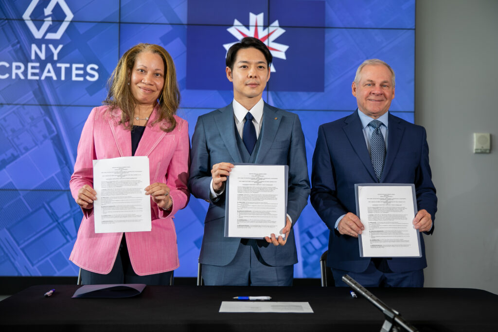
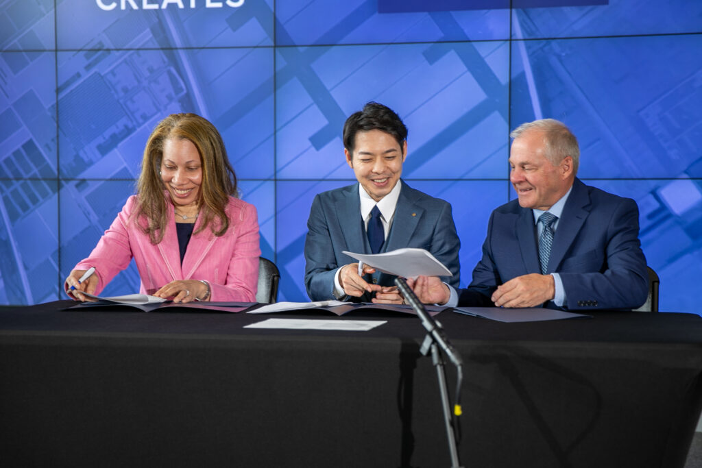
Albany, N.Y. – The New York Center for Research, Economic Advancement, Technology, Engineering, and Science (NY CREATES) announced today it has been awarded a $4.7 million grant from the National Science Foundation (NSF) to support the establishment of the Education Alliance for Semiconductor Experiential Learning (EASEL) program. This workforce development initiative aims to help address the growing national demand for a skilled workforce in the semiconductor industry, a critical need highlighted by the U.S. CHIPS & Science Act.
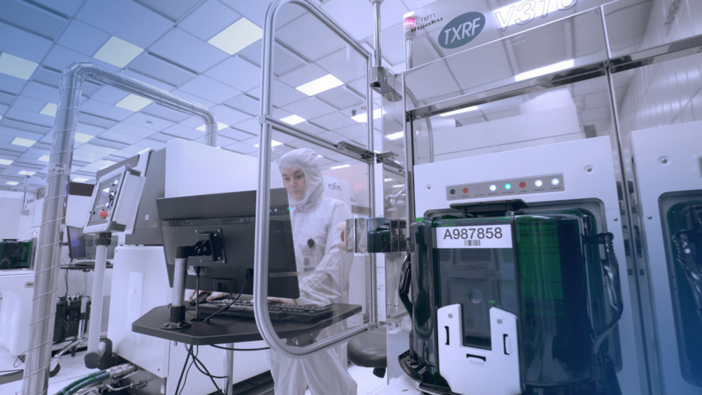
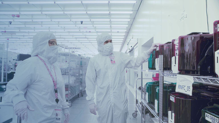
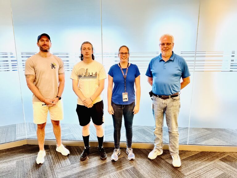
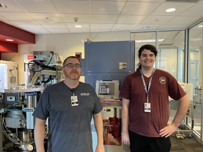
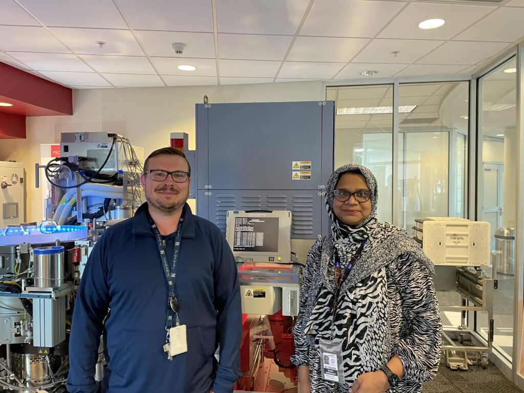
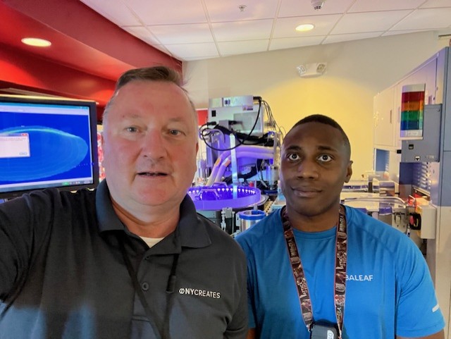
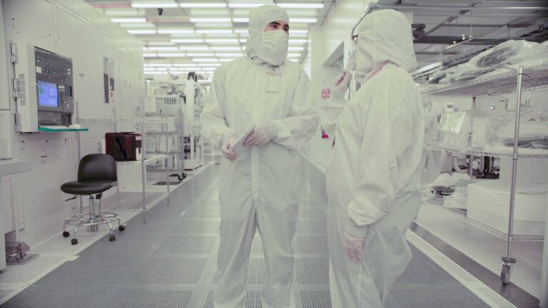
The U.S. CHIPS & Science Act, a transformational investment in the nation’s semiconductor industry, will help create an estimated 280,000 jobs across the computer chip industry, with nearly half of those positions requiring skilled technicians. EASEL will play a pivotal role in filling these technician positions by providing hands-on, immersive learning experiences for college students from across the U.S. at NY CREATES’ Albany NanoTech Complex to help them hit the ground running in semiconductor careers. EASEL will also provide similar experiences to teachers and instructors to better prepare them to educate the nation’s semiconductor workforce.
Senate Majority Leader Charles Schumer said, “This $4.7 million from my CHIPS & Science law will help college students from across America come to Albany NanoTech to get hands-on training and become the next generation of America’s semiconductor workforce. It will bring together community colleges, including Onondaga Community College, who are launching chip technician programs now and give them access to the most cutting-edge research facilities to get them ready for good-paying jobs at companies like Micron and GlobalFoundries. I crafted this law with Upstate NY as my north star, because I knew that with targeted federal investments like this, the communities in Upstate NY that powered America’s industrial past could be the ones to build its future and bring critical manufacturing back from overseas to America. Together, we’re boosting Upstate NY as the heart of America’s semiconductor manufacturing industry. I’ve worked closely with the Administration, including the NSF, to make the case for federal investment in Upstate NY’s R&D and workforce training programs, and I’m grateful that the NSF recognizes Albany NanoTech’s premier work and leadership in boosting the nation’s semiconductor industry.”
Senator Kirsten Gillibrand said, “This is a long overdue investment in one of the Capital Region’s most important bridges. I’m proud to have fought for federal funding for this project and will continue to fight for every dollar necessary to get this restoration done.”
“We are thrilled to receive this grant from the NSF to further train a robust semiconductor-focused workforce,” said NY CREATES President Dave Anderson. “We look forward to engaging with our industry partners, including Micron and GlobalFoundries, as well as with our initial cohort of academic institutions to connect students with this program. Providing them the vital skills required to contribute to this area of research, development, and manufacturing is critically important for New York State and the U.S., especially given the exciting promise of the U.S. CHIPS & Science Act which is already driving industry expansion.”
“I consider myself lucky to represent a region that is such a strong leader in the semiconductor industry, from manufacturing facilities and research and development programs to our cutting-edge educational institutions,” Congressman Paul Tonko said. “I’ve been immensely proud to lead efforts in the House on CHIPS & Science Act funding and bolstering our semiconductor ecosystem because I know how important this issue is—not only for our national security and economic competitiveness, but also for creating good paying jobs here at home. This grant only furthers our Capital Region’s leadership role by driving further education and training for students looking to enter into this growing industry. My congratulations to NY CREATES on leading this exceptional project.”
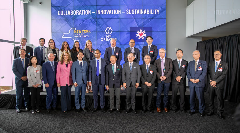
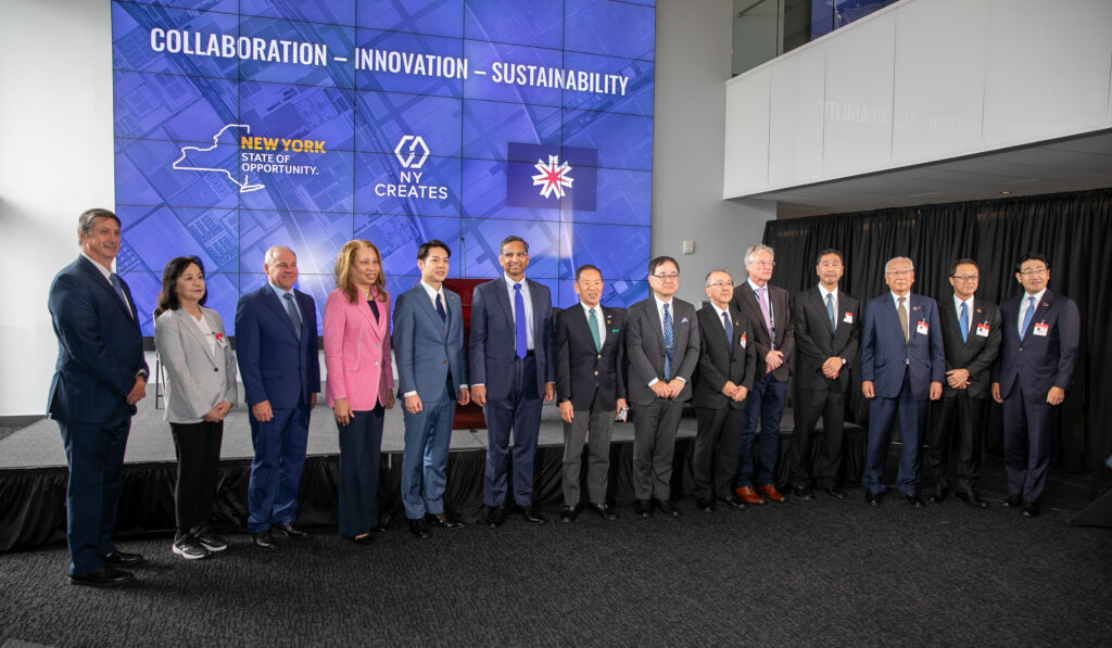
The EASEL program will bring together a coalition of community colleges and leading U.S. semiconductor manufacturers to develop and implement multi-modal experiential learning opportunities. Initially, the alliance will include four core community colleges—Columbus State Community College, Onondaga Community College, LaGuardia Community College, and Madison Area Technical College—and will expand to include additional institutions across key semiconductor manufacturing regions in the U.S.
“The SEMI Foundation is proud to support initiatives like the EASEL program that strengthen our initiatives cultivating the next generation of semiconductor professionals,” said Shari Liss, Executive Director of the SEMI Foundation. “By bridging academia and industry, this program will provide students with the hands-on experience and technical skills they need to thrive in a rapidly evolving field. Collaborative efforts like these are key to ensuring the continued growth and innovation of the semiconductor industry in the U.S.”
“NY CREATES plays an important role in Micron’s workforce development strategy, and we’re thrilled this NSF grant will expand access to semiconductor skills and training at NY CREATES’ Albany NanoTech Complex,” said Micron Chief People Officer April Arnzen. “The CHIPS & Science Act has propelled the growth of the domestic semiconductor industry, and Micron is committed to cultivating a diverse, highly skilled workforce that can support advanced memory manufacturing alongside our partners, including NYCREATES and Onondaga Community College. We look forward to the rich experiences students and faculty will gain from this hands-on programming.”
“Essential chips are strengthening supply chains and driving innovation. To continue growing, our industry must work together to inspire and develop tomorrow’s skilled semiconductor workforce,” said GlobalFoundries Chief People Officer Pradheepa Raman. “Building a robust and diverse talent pipeline requires strong public-private partnerships. We are proud to deepen our collaboration with NY CREATES, NSF and others on these critical workforce development efforts.”
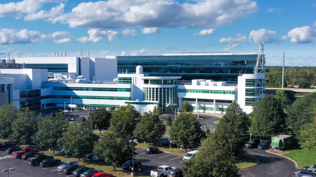
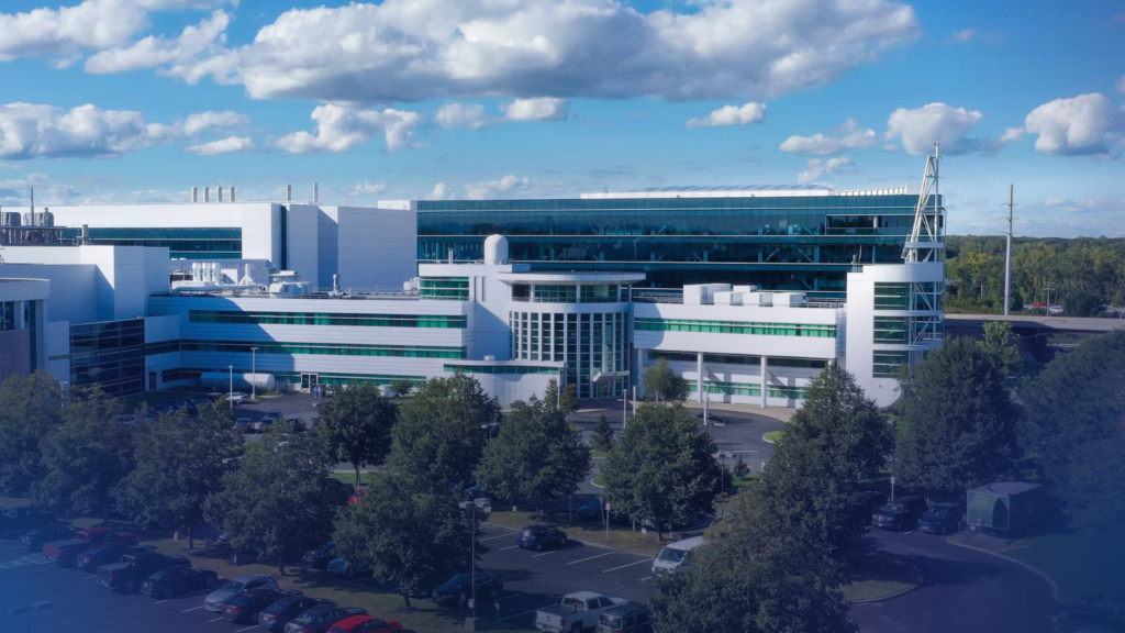
Over the course of the four-year project, EASEL is expected to support up to 660 student learners and faculty participants, providing over 43,000 hours of immersive experiential learning and 4,000 hours of faculty technical development. The project will leverage the unique capabilities of NY CREATES, which operates the largest non-profit 300mm semiconductor R&D facility in North America, offering a complete integrated circuit process flow down to the 5-7nm device node.
This award from the NSF underscores the importance of workforce development programs that can scale to produce skilled technical workers. This is especially important as NY CREATES’ Albany NanoTech Complex growth continues, further expanding its capacity with its High NA EUV Lithography Center, currently under construction, which can provide a neutral location to support a future National Semiconductor Technology Center under the U.S. CHIPS & Science Act.
###############
About NY CREATES
NY CREATES serves as a lab-to-fab bridge for advanced electronics, fostering public-private and industry-academic partnerships for technology development and innovation. NY CREATES attracts and leads industry-connected innovation and commercialization projects that secure significant investment, advance R&D in emerging technologies, and generate the jobs of tomorrow. NY CREATES runs some of the most advanced facilities in the world, boasts more than 2,700 industry experts and faculty, and manages public and private investments of more than $20 billion—placing it at the global epicenter of high-tech innovation and commercialization. Learn more at www.ny-creates.org.
###
Media Coverage:
Times Union: NY CREATES gets $4.7 million National Science Foundation grant