
Dr. Tristan Meunier, CNRS – Néel Institute
The Quantum Spin Grenoble Initiative For Large Scale Quantum Computing
November 18 (Thursday), 2021
The Quantum Spin Grenoble Initiative For Large Scale Quantum Computing
November 18 (Thursday), 2021
Quantum Sensing in the Hidden Sector
November 4 (Thursday), 2021

Quantum Point Defects for Quantum Network Applications
October 21 (Thursday), 2021

Quantum Information Processing with Semiconductor Quantum Dots
October 7 (Thursday), 2021
Scaling Photonic Quantum Computers
September 23 (Thursday), 2021

Innovations to Enable Future Logic Scaling
September 9 (Thursday), 2021
Nanocomputing, Neuromorphic Computing and Quantum Information Science Technologies at the AFRL Information Directorate
August 26 (Thursday), 2021

So You Wanna be a Deeptech Entrepreneur?
Aug 12 (Thursday), 2021
Power Electronics Technology for Tomorrow’s Solutions
July 29 (Thursday), 2021
Ultra-Wide-Bandgap Semiconductors – Challenges and Opportunities
July 8 (Thursday), 2021
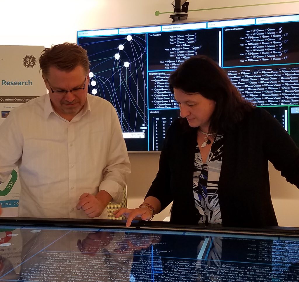
Quantum Annealing Applied to an Industrial Problem
June 3 (Thursday), 2021
Integrated Quantum Information Platforms at MIT Lincoln Laboratory
May 20 (Thursday), 2021
Band Superconductivity in Periodic Constricted Nanoribbon Structures
May 6 (Thursday), 2021
Integrated Multi-wavelength Control of Ion Qubits
April 22 (Thursday), 2021
Toward a Quantum Enhanced Microscope for Imaging Biological Systems
April 8 (Thursday), 2021
The “super” Superconducting Josephson Junction Non-linear Oscillators
March 4 (Thursday), 2021
Quantum Computing with Atoms
February 4 (Thursday), 2021
Quantum Networking at the AFRL Information Directorate (Rome, NY)
January 21 (Thursday), 2021
Semiconductor Process Needs for 5G and AI
January 14 (Thursday) 2021