RESEARCH
The NY CREATES R&D team shares with our partners a zest for innovation, and a drive to break new ground every day. We are working with partners in industry, national labs, and academia on research efforts that are yielding significant advancements in many technology and industry sectors. In addition to the concise descriptions below, the Resources page provides links to journal articles that dive into the details of our work in these areas. In addition, NY CREATES hosts the Emerging Technologies Seminars roughly twice each month, featuring accessible presentations by leaders from across the globe. Topics range from photonics to power electronics, from artificial intelligence to quantum technologies, from advanced CMOS to nano-biological devices – all areas of interest to NY CREATES!
 Neuromorphic computing systems approach information processing in a fashion inspired by how we understand the human brain to function. The traditional ‘von Neumann’ computer architecture, with memory separate from logic circuits is dispensed with, in favor of an architecture that uses nanofabricated structures called ‘memristors’ for data processing in an energy efficient fashion.
At NY CREATES, neuromorphic computing technology development includes resistive-random-access-memory (ReRAM) structures integrated with 65nm CMOS transistors, superconducting optoelectronics that utilize Josephson junctions and cryogenic Si-based light emitters, as well as photonic integrated circuits. Our partners include both commercial entities, universities and national labs.
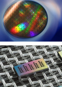
Photonic integrated circuits (PICs) are being deployed in an increasing range of applications where speed and energy efficiency is important – traditional electron-based wiring suffers from “RC delays” and energy loss due to “parasitics”. Data communications between IC chips to those between large-scale data centers use PICs enabling terabit per second speeds. PICs have been used as matrix multiplication accelerators, and in artificial intelligence schema. Autonomous vehicles will increasingly use photonic integrated circuits for LIDAR systems that do not have any moving parts that are inherently less reliable.
The innovation and value-add
provided by the team of integrated photonics experts at NY
CREATES is bolstered by one of the nation’s leading Test, Assembly and
Packaging facility (TAP) in Rochester, NY. Packaging of photonic and electronic
devices is an increasingly complex part of the finished product and can make up
more than three-fourths of the finished component cost. Excellence in advanced
packaging is critical for many applications including information processing,
telecommunications and data communications, biological and chemical sensing,
and control systems for autonomous vehicles.
The TAP facility provides a critical complement
to wafer fabrication operations in Albany, allowing partners the ability to
undertake industry-leading work on wafers and chips, unparalleled to other
global fabrication facilities. The TAP facility is part of AIM Photonics, a U.S. Manufacturing
Innovation Institute. Learn more about TAP’s state-of-art
toolset and flexible processes at the AIM Photonics website
Qubits, or quantum bits, are harnessed in areas such as quantum computing, quantum communications and quantum sensing. Qubits have been created in a variety of modalities (including superconducting, trapped ion, Si-based spin, and photonic qubits) – each with unique advantages and challenges. Electromagnetic and gravitational field sensing using qubits, quantum signal transduction (transferring the quantum information from superconducting qubits to photons, say), as well as the means to prepare, manipulate, and read-out qubits, fall into the broad (and growing) area of quantum technologies.
The team at NY CREATES has been engaged in demonstrating qubit fabrication using state-of-the-art wafer processing tools, in order to improve the ultimate performance of quantum technologies. Research and technology development for superconducting qubits, single flux quantum circuit elements, superconducting nanowire single photon detectors used in photonic quantum computing and elsewhere, interfaces to trapped ion qubits, and their integration into larger systems is part of the mandate of NY CREATES’ research team. Our partners include National Labs, industry and university researchers.
View videos of our presentations at Q2B 2021 here
This link will take you deeper into our work on quantum technologies!
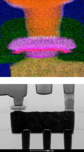
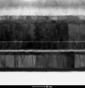
 Magnetic Random Access Memory (MRAM) is an emerging memory technology that can be seamlessly integrated into advanced CMOS technology nodes. MRAM is being explored by many companies and researchers worldwide due to its promise as an inexpensive, fast, energy efficient, and non-volatile memory technology. This technology is also seen as a potential enabler for stochastic neural networks and ultra-efficient exascale computing at cryogenic temperatures. NY CREATES researchers are partnering with a variety of commercial entities to develop scalable MRAM devices using advanced lithography and other leading edge process capabilities in NY CREATES’ facility at Albany, NY.
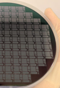
The ubiquitous information processing needed by society in the next decade or two relies on process technologies that yield devices with game-changing performance in energy efficiency and speed. Each individual process technology is developed and coupled with upstream and downstream steps to enable the fabrication of advanced devices. New applications require researchers at NY CREATES to re-tailor processes and their integration to satisfy unique or more demanding requirements. NY CREATES, in partnership with universities and semiconductor-related companies on site and elsewhere, has successfully developed novel structures and devices with applications ranging from 5nm-node CMOS and 2D-channel transistors to augmented reality. Expert technologists at NY CREATES have enabled material and equipment suppliers to develop, test and refine their offerings to their customers in the IC fabrication industry across the world.
 The field of power electronics has been supercharged by the growing adoption of wide bandgap materials such as SiC and GaN, among others. Power electronics capable of handling higher voltages and currents, and operating at higher frequencies have enabled designers to dramatically shrink the size of components and increase the overall energy efficiency of the system. Power electronics of smaller size and higher efficiency are critical in the growing sectors relating to renewable energy sector, electric cars and locomotives, and communications.
NY CREATES is proud to partner with companies such as Danfoss and Cree who have recently established growing operations in upstate New York for power electronics packaging and for SiC device fabrication respectively. NEXGEN Power Systems is based in a NY CREATES facility in Syracuse, NY where it is engaged in developing GaN-on-GaN devices for a range of applications demanding smaller, light-weight, and energy-efficient power electronics.
Heterogeneous integration, 3D and 2.5D integration, and interposers are technologies that are becoming increasingly important to address the need to build smaller and more efficient systems that encompass broad functionalities. 3D and heterogeneous integration enable Si, photonic, III-V, and wide-bandgap material chips to be yoked together with high bandwidth channels while contributing the native strengths of each chip technology to the system. 3D integration at NY CREATES’ Albany site includes work on both ‘die-to-wafer’ and ‘wafer-to-wafer’ configurations. Experts at Albany have worked over the years to advance 3D integration technologies, such as Cu/Cu bonding (as part of SEMATECH’s 3DI Enablement Center), and oxide-oxide bonding utilized in AIM Photonics offerings.

