Harnessing 193nm Optical Lithography
In partnership with Dr. Kevin Osborn and his team members (Dr. Neda Foroozani and Dr. C.C. Hung) at University of Maryland, the Albany team characterized transmon qubits fabricated using 193nm optical lithography on 300mm silicon wafers. The resulting qubits exhibited good energy relaxation (“T1”) times of around 25 microseconds. Long enough energy relaxation and phase decoherence times are needed in quantum computing systems to permit longer chains of qubit operations to be performed before inevitable errors creep in. In addition to long qubit coherence times, tight control of the qubit frequency is useful to enable large scale quantum systems to be built, by avoiding ‘frequency collisions’, and possibly reducing the complexities introduced by needing to nudge each qubit’s frequency into place individually.
In this work, 193nm optical lithography was used for the first time in the world to form the Dolan bridge. While the Dolan bridge approach has been widely used for superconducting qubit fabrication, it typically involves electron-beam lithography. In electron-beam lithography, each feature is individually written by rastering an electron beam over the surface of the wafer – which necessarily limits the speed and is known to introduce variability when such patterns are to be replicated across a 300mm wafer. In contrast, the optical lithography techniques that have been honed over the past several decades in the IC industry permit much larger areas to be simultaneously patterned by precisely chosen wavelengths of light – in our case 193 nm. The lithography equipment and associated materials have been optimized to achieve tight control of feature dimensions across the wafer, down to single nanometers, and the less than 1 % standard deviation in lithographic feature width reported. Such control in feature dimensions across the chip was essential in achieving the qubit frequency control demonstrated in this work.
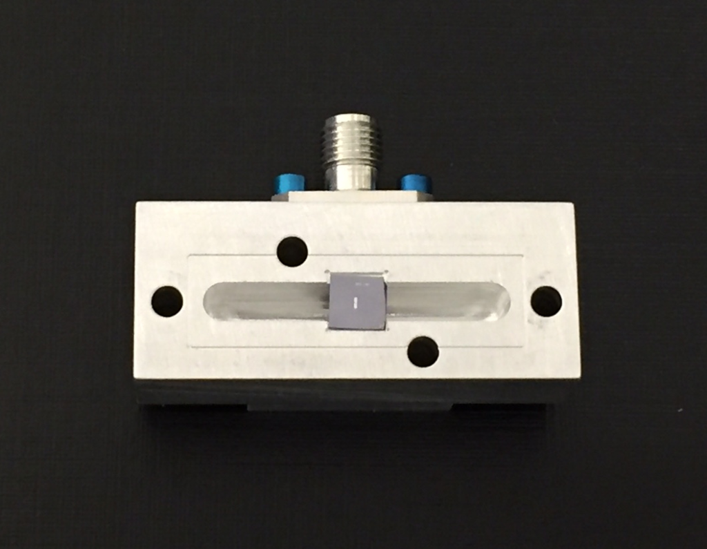
It should be noted that after e-beam lithography, the wafer was cut into smaller die, in order to accomplish the shadow evaporation of aluminum, and the in situ formation of the required aluminum oxide tunnel barrier. The shadow evaporation was conducted at the Shared Instrument Lab at the University at Buffalo, NY. Ongoing work by the NY CREATES team aims to eliminate the need for shadow evaporation with a redesign of the process flow so that high quality qubits can be fabricated across a whole 300mm wafer, utilizing 193nm optical lithography along with chemical mechanical planarization and other processes using state-of-the-art 300mm process tools.